CATEGORIES
Optical Thin Films
The primary reason for coating surfaces with optical thin films is to modify their reflection or refraction properties, mostly through interference processes. Optical thin films often consist of stacks of layers with alternating refractive index. These layers are often ceramics such as Al2O3 or SiO2. The 2D parameters that determine the optical properties are refraction index, thickness and absorption coefficient. Other factors such as the wear or scratch resistance, the environmental stability and so on may play a role as well too, but we will not highlight those here. As we saw earlier, dense thin films such as ECR plasma coated films are generally superior in their environmental suitability than columnar low-energy-coating thin films, which are porous.
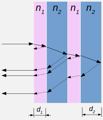
Diagram of a dielectric mirror in which thin films with alternating refractive indexes are stacked. The path lengths of the reflected light rays differ by exactly one wavelength of the light, which leads to constructive interference.
Material Properties
While the thickness of the layers is determined by the coating process, the absorption coefficient and the refraction index are both material properties which in theory cannot be willfully manipulated by coating tool adjustments. Yet, the dependence on the coating tool is very real. The optical properties of one and the same material can widely vary depending on the coating process.
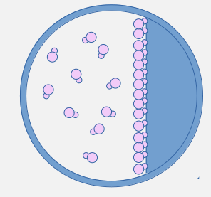
Although certain properties can be intentionally sought for certain applications (catalyst surfaces for instance), low energy coating leads to columnar growth, low density, plenty of interstitial space and hence the optical properties, especially regarding the refraction index, will strongly deviate from the theoretical values. Another problem is that the interstitial space stores humidity and other contaminants, which in turn will change the optical properties in a rather uncontrolled fashion depending on environmental conditions.
Using coating tools with ion beam assistance that provides energy to the film by bombarding it with accelerated particles may likely come along with unwanted side effects, such as preferential sputtering of one of the thin film components, incorporation of noble gas atoms and damage to the underlying substrate. The preferential sputtering may lead to a deviation from the stoichiometric composition. For ceramic materials that means, that the thin film will have a slight metallic character and hence a noticeable absorption coefficient. The damage to the underlying substrate will likely roughen the interface between the layers, and will even cause unwanted intermixing of layers with unknown conditions. For edge-emitting laser diodes, the interface between the semiconductor and the facet mirrors is one of the main weak points leading to CODs and hence very susceptible to unwanted ion incorporation or otherwise damage of the lattice.
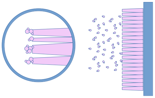
In the upper figure we in a close-up of the growing film how low energy coating leads to columnar growth. This porous structure is linked to smaller refraction indexes than the theoretical value. If the incoming species to the thin film carry a lot of kinetic energy (lower figure – close-up), they bombard the film that they are creating. While this dismantles the columnar structure and helps creating a densely packed film, it also damages the underlying substrate and creates unwanted defects in the growing film.
Thickness Control
The thickness is a function of the coating time and the growth rate. The latter can become a very complex and wild figure, since it depends from many partly interdependent aspects with non-linear behavior.
On the generation of species side, the thin film growth rate depends of the sputter rate, which in turn depends from the target material hardness, the wattage of the sputter RF field and usable target size. It needs to be noted, that the hardness of the target drastically increases when the metal surface becomes poisoned in a reactive process and that the target usage changes its geometry and often its available surface and ejection angle.
On the transport aspect, the growth rate depends on the fraction of the sputter species that are ejected or otherwise accelerated towards the substrate and not deviated by random collisions with the background gas. Depending on the tool configuration, much of the sputtered material will not land on the substrate but elsewhere in the chamber and needs to be cleaned up regularly. The ECR plasma sputtering tools from JSW Afty are configured in such a way, that most of the ejected material does land on the substrate or on easy to clean surfaces.
A low background gas pressure increases the growth rate. The geometrical aspects of the tool on the other side are a constant. The location of the substrate in relation to the substrate as well as the acceleration direction of the sputtered species will influence the growth rate and the gradient of the growth rate over the substrate area. A high homogeneity allows for larger surfaces to be coated at once. To increase the homogeneity, the substrates are often spun during the coating. The growth rate on the substrate is reduced by desorption of species that reach the substrate but depart if they have too much energy. Also sputtering of the growing film by impinging species reduces the growth rate.
The maximum area in the substrate that can be coated with a certain degree of homogeneity in the thickness and stoichiometric is an important figure of merit for a coating tool. It is defined by the maximal percentage variation of thickness along a certain area. For instance max. 3% over a diameter of 8 inches would be a typical value for an ECR plasma sputter coating tool.
The growth rate does have a significant influence on the crystal structure of the film. The main reason is that the incoming species do not have time or physical space to settle down in their preferential lowest energy spot, even if their adatom mobility is high. When too many species arrive too quickly at once, they hinder each other in their mobility. This can be also be seen in variations of the intrinsic film stress as well.
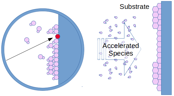
ECR plasma sputtering provides the impinging species with just enough kinetic energy to overcome columnar growth. The energy transfer through excited electrons increases the adatom mobility, promoting dense tight packing growth. High energetic ion implantation, physical etch of the underlying substrate can be kept to a minimum.
Stoichiometry Control
Optical films are desired to have very low absorption coefficients. Zero is best actually. Different ceramic materials are used because they are transparent in different wavelength ranges, theoretically. Yet, the coating needs to ensure that the films are fully saturated with oxygen or nitrogen to actually meet the theoretical value for the absorption coefficient. Otherwise, loose metal ions will increase the optical absorption of the film – throughout a wide range of wavelengths. Even if the coating is done with a ceramic target, which is unusual, a partial pressure of oxygen or nitrogen is always added to the Ar plasma to ensure saturation. Most of the times though, the film is grown with a metallic target and the incorporation of the nitrogen or oxygen is done through reactive sputtering. Since the lighter oxygen or nitrogen has a somewhat larger tendency to be ejected from the growing film than the metal atom, providing an oversupply of reactive agents makes sure that all the metal atoms are saturated in the thin film.
A surplus of reactive agent does not pose any problem to the growing film but depending on the system it can poison the target, with all the inconveniences carried along by that. The additional reactive agents that are not utilized mostly remain in the gas phase until removed from the chamber by the pump.
While keeping the absorption coefficient close to zero, the refraction index can be modified at will within a certain range by modifying the O2/N2 ratio and creating mixed species such as SiOxNy. Like this, the diffraction index can be modified from the n=1.6 of SiO2 to n=2.0 of Si3N4 gradually and reliably. Using silicon as the metal part is just an example. The O2/N2 ratio can be adjusted very precisely with the MFCs. Even rugate filters (with gradually periodically varying refractive index) and many other highly complex layer stacks with or without gradual transitions can be reliably manufactured with ECR plasma sputtering tools in this way.
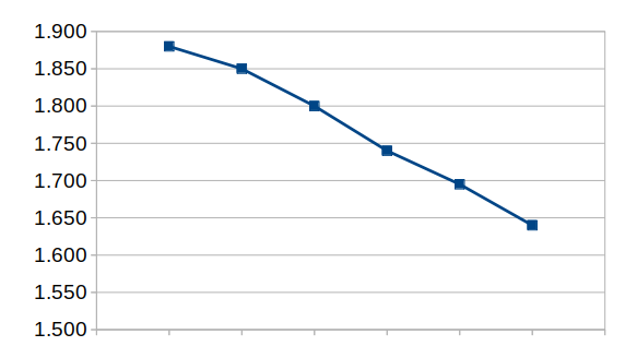
Varying the refractive index of a SiOxNy film with varying x/y ratio processed in the same ECR plasma sputter tool by just varying the O2 to N2 flow ratio.
Inline Monitoring
Deposition tools with Kaufmann type ion beam guns do experience a shift in the deposition parameters due to the inevitable wear of the gun electrodes and/or grid holes.
In many cases the plasma activity on the target is not homogeneous, but has limited areas with highest activity. The irregular erosion of the target creates mountains and valleys in the used-up target. Sometimes these are referred to as race tracks because of how they look like. The inhomogeneous erosion leads to gradual modifications in the direction and energy distribution of the sputtered species, leading to a slightly different geometric arrangement.
Therefore, live monitoring of the thin film growth properties such as refractive index and thickness (often with a piezocrystal that changes its resonant vibration with the thickness of the coating) is used to monitor the varying deposition rates. In some cases laser light is a good method to analyze the stoichiometry of the film by spectral analyzing of the reflected light.
The ECR plasma coating tools do need more elaborate plasma sources without electrodes but seem to be more constant and the process parameters very reliable, robust and reproducible, which usually eliminates the need for live monitoring of the thin film growth. The geometric arrangement of the plasma sources and the separation of
different energy sources for different generation stages of the plasma
and the sputtering process allows to a high degree of process control. This translates in a high reliability and dependability in the deposition characteristics and growth rate that do not vary from wafer to wafer.
In ECR plasma coating tools barely routine sample checks after the coating are sufficient to monitor the coating behavior.
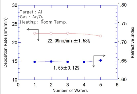
ECR plasma sputtering wafer-to-wafer uniformity.
Do you like what you see?
We value your feedback, so let us know what you think!
Let us also know which topics you would like to see expanded.
Just give us a call, send us an e-mail or use the form to contact us.