CATEGORIES
Reactive Plasma Cleaning
After loading the substrate into the coating chamber but prior to the actual thin film growth it is worth-it to pay attention to the substrate surface itself. Even if the substrate has been chemically primed prior to loading, a native oxide layer plus monolayers of humidity, organic monolayers or other unwanted rests from the previous process can often be found on the substrate. These will strongly influence the thin film properties and lower the adhesion and the electric contact of the thin film to the substrate.
An in-situ cleaning step consisting of treating with a (reactive) plasma is a common strategy to clean the substrate and prepare its surface for the subsequent thin film deposition. Reactive plasma cleaning relies on the formation of volatile reaction products of the contaminant at low temperatures. Oxygen or hydrogen can be used for reactive plasma cleaning and they are very effective in removing hydrocarbons and adsorbed water vapor from the substrate surface.
Reactive plasma cleaning is typically performed at gas pressures of 0.1×10⁻³ – 0.7×10⁻³ mbar, usually using an AC excited plasma. The reactive gas can be oxygen or air (21% O2) for cleaning surfaces that can withstand oxidation, or can be hydrogen or forming gas (90% N2 :10% H2) for those that require a non-oxidizing environment. The surfaces to be cleaned are often placed in a region outside the plasma generation region (i.e. remote plasma region).
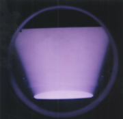
Reactive plasma at work. The substrate is placed within a volume rich in highly reactive ions that will render organic compounds volatile and combust them away without a trace.
Cleaning Facets for Edge Emitting LAsers
For edge-emitting laser diodes, this is a crucial topic, since the interface of the semiconductor to the optical coating will be key for the capability of the laser diode to handle high laser power.
As already pointed out on another wiki, in edge emitter laser diodes that have been cleaved, the native oxide layer that builds on the dangling bonds of the interrupted crystal lattice can pose a reliability weakness: When the laser light, which is bouncing back and forth in the transparent semiconductor, is significantly absorbed at the surface oxide layer, heating up and leading to an irreversible catastrophic optical damage.
Each laser diode type has a different treatment process for the cleaning of the facets to remove any native oxide layer.
Depending on the desired substrate surface modification different techniques can be applied. Also some treatments can only be done outside of the coating tool. Nonetheless the application of a glow discharge and the bombarding with gas ions can usually be performed in the same coating chamber and/or are easy enough to integrate with a coating system. The advantage is that the substrate is not exposed to the atmosphere after the surface treatment and the coating can begin right away on the prepared surface. Clean surfaces are very reactive and easily recontaminated.
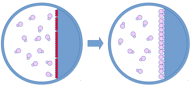
Also non reactive plasma, such as pure Ar can be used: The sputtering effect of the ions hitting the substrate will produce a cleaning effect by removing the first layer of the substrate (including the contaminants on the surface). Unfortunately it is also possible that the used gas for the sputter effect is incorporated in the top nanometers of the substrate and creates defects in the lattice of the semiconductor.
ECR plasma sputter reactive coating of Al2O3 might just have the right mix of low impact energy and high adatom mobility through the energetic electron heating to promote an incorporation of the native oxygen into the growing Al2O3 without damaging the underlying semiconductor by the bombarding species.
If the incoming species to the thin film carry a lot of kinetic energy, they bombard the film that they are creating. While this dismantles the columnar structure, it also damages the underlying substrate and creates unwanted defects in the growing film.
Do you like what you see?
We value your feedback, so let us know what you think!
Let us also know which topics you would like to see expanded.
Just give us a call, send us an e-mail or use the form to contact us.