CATEGORIES
Substrate and Low Energy Settings
Substrate is the used designation for the area where the thin film grows. This is the final goal and hence the most important part of the whole process. In this area, the particles sputtered from the target will nucleate on the surface as they arrive and grow the film by a number of processes. The most basic principle is that incoming atoms or molecules are adsorbed by the substrate or coalesce with already adsorbed molecules of the same material. If only low energy deposition processes are involved, a columnar film structure is often the result. The reason is the microscopic roughness of the substrate leading to a preferential adsorption by the portions of the surface spots laying higher. As soon as an atom or molecule is adsorbed it has no remaining energy to overcome the adsorption bond and move somewhere else. Hence, the columnar growth that originates on top locations trapping the atoms will proliferate (see figure). Columnar structure is not very good for optical thin films due to its low density and the interstitial spaces that allow contaminants and air humidity to alter the optical and insulation properties of the coated surface.
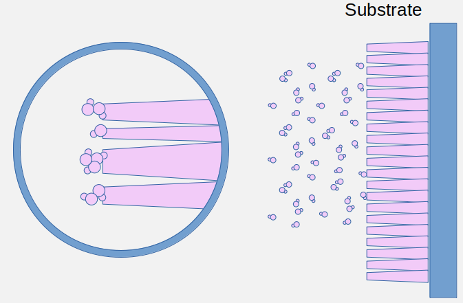
Close-up view of columnar growth, which is often the result when the atoms attach to the first possible spot that comes along in their path. Once the atom “touches ground” there is no additional energy to move around and form a more dense crystalline structure. There are advantages to this type of coating, such as high throughput.
Adding (Too Much?) Energy to the thin film
By providing energy to the growing film, the adsorbed atoms and molecules become able to slightly roam around their growing position to search the lowest energy spot. The result is a film with much higher density much closer to a crystalline solid instead. Optical films with dense structures are preferred since they are mostly inert to interaction with the environment. They offer a good sealing and do not change their physical properties with varying environmental parameters.
The required energy to increase the atom mobility in the growing film can be provided by heating the substrate, but this could lead sometimes to a damage of the underlying materials. In many cases there is a maximum temperature to which the substrate may be heated and therefore not commonly applied to protect delicate devices. Another way to provide the energy is by increasing the kinetic energy of the incoming sputtered species. This is a very common method for optical thin films. The energy of the sputtered species themselves can be large enough in some cases. In other cases, an additional Kaufmann type ion gun is used to accelerate ionized Ar atoms towards the substrate (Ion Beam Assist).
Just by increasing the target sputter energy, the ejected particles arrive at the substrate with relatively high kinetic energies and the deposition process becomes very complex. Some of the incoming particles are implanted in the top nanometers of the substrate while others are backsputtered. An etching sputter effect of the underlying layers is common as well. Already coalescing film is bombarded by the new incoming species and the initial columnar structure is dismantled by the impinging atoms.
While the incoming high energetic ions do provide thermal energy for the adatom mobility, they also create unwanted damage. Crystal defects, implanted particles, shadowing, redeposition of ejected particles and in the case of materials with more than one species (every insulator for instance) selective sputtering (one of the species is more prone to be ejected from the growing film by the incoming projectiles than the other, leading to an stoichiometric imbalance) make it rather impossible to model the thin film growth in exact detail. Common energies for the incoming ions for ion beam sputtering tools can be found in the range of 100eV and above.
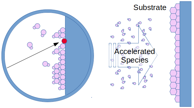
If the incoming species to the thin film carry a lot of kinetic energy, they bombard the film that they are creating. While this dismantles the columnar structure, it also damages the underlying substrate and creates unwanted defects in the growing film.
The middle way of ECR plasma sputter coating
In the case of ECR plasma coating, the energy for the substrate is provided by a combination of bombarding the growing film with relative low energy sputtered species (below 30eV) and by a large quantity of hot electrons from the ECR plasma. The electrons do not have a significant kinetic energy due to their extremely low mass, yet their energy transfer to the growing film is very efficient and their sheer quantity succeeds in transferring thermal energy to the film, increasing the atom mobility without creating unwanted lattice damage.
The large amount of energetic electrons available and the ability to reduce the sputter energy independently of the plasma energy are key features of the ECR plasma technology that lead to these fantastic thin film properties.
For this reason, it is not possible to use the ECR plasma tool to physically etch the native oxide layer of the substrate that is always present on the substrate. Instead, due to the available energy, the native oxide smoothly incorporates into the first optical layer which is most likely an insulator such as Al2O3. The interfaces between layers deposited with ECR plasma coating tools are very smooth and the transition is sharp, without intermixing of layers yet good interlayer adhesion.
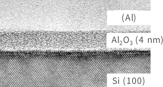
Cross sectional TEM image of an Al2O3 film with a tiny yet extremely homogeneous and dense interface to the other layers Si and Al. Coated with an ECR plasma sputter coating tool.
Do you like what you see?
We value your feedback, so let us know what you think!
Let us also know which topics you would like to see expanded.
Just give us a call, send us an e-mail or use the form to contact us.