CATEGORIES
Creating The Facets
What's Next?
The laser diodes we are describing here are edge emitters and while dicing the wafer into individual laser diodes we are also creating the resonator cavity. Mirror-like facet quality as well as exact parallel facets are very significant contributors to good reflective properties and operational reliability of the lasers. To achieve this, the well established method of scribe and break is very popular because it takes advantage of the crystal structure itself and allows the semiconductor to cleave along the crystallographic planes, that are naturally smooth and parallel. The mirror facets play a central role in the long term operation reliability of the lasers. Hence, in most cases, additionally to perfectly cleaved facets a plasma deposition step is necessary to enhance and tailor their properties.
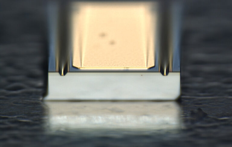
It is rather impossible to dice such smooth facets. They are cleaved in a similar way as diamonds are.
Letting it Naturally Break
Since we do not want to actually forcefully cut through the semiconductor and damage the facet, but rather “induce” it to fracture where we would like it to fracture, while conserving its crystal quality, there is a certain portion of the process that defies our control. This is cumbersome to many but does require to learn which are the parameters that we can control and where the ‘magic’ or ‘artistic’ part comes in.
With the scribe and break tools there are ways to increase the success rate and hence the yield by mastering the process. Year long experience does play a role for this type of process but there are some factors to consider no matter if you are a beginner or a seasoned expert.
The success rate depends on the depth of the inflicted damage (d) and the thickness of the wafer (t), where a large ratio of d/t translates into a high breaking yield. The inflicted damage can be the depth of a median crack in the case of a diamond scriber or the depth of a cut in the case of a laser scriber.
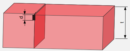
In this model of an edge-emitting laser diode, the thickness of the substrate is depicted by t and the thickness of the inflicted damage is d. In the case of a diamond scriber d would be the depth of the median crack (not the depth of the diamond damage). In the case of a laser scriber, d is the depth of the ablated material or laser inflicted kerf.
The Thickness of The substrate and the Chip size
In a practical sense, limiting the maximum thickness of wafers also increases the chances of success. Wafers for laser diodes are normally thinned and polished down to 100µm or less, which is an elaborate but rewarding processing step. A thin semiconductor is an aid for the thermal cooling on the laser as well, although admittedly, this is usually less of a concern if high mobility substrates such as GaN are used, or if the laser is bonded upside down, with the epitaxial layer laying directly on the cooling sink. Another limitation specifically linked to the use of scribe and break is the device size. The ability to break by applying pressure is proportional to the size of the device. It can become very difficult to achieve high yields if the device sizes are below a certain figure. 150µm seems to be a lower limit for device lateral size since this is also already in the range of the device thickness.
The process of dicing chips through scribe and break is somewhat relatable to a commonplace experience: Breaking chocolate chunks from a chocolate bar. The bar is grooved in the individual bites for ease of breaking. This would symbolize the scribes. The actual breaking happens through a bending force. It is obvioulsy easier to break it if the groove is deep and the bar is thin. It is as well easier to break larger chunks than small pieces. This applies to breaking semiconductors as well.
Crystal Plane Orientation
The most obvious requirement related to scribe and break is the necessity to align the cleaving streets with the crystal planes. GaAs devices are commonly produced in the <100> crystal plane configuration, giving the optimum orientation in terms of electronic properties in the wafer surface. Coincidentally, this allows for straight fractures to be made in the {110} set of planes. These planes are at right angles to the <100> surface and to each other. Therefore, in the case of GaAs and its related compound InP that both share a zincblende crystal structure these limitation does not pose any disadvantage at all. The same can be stated to InP.
For the zincblende structure of GaAs and InP it is customary to prepare wafers that are in the <100> orientation. The crystal planes are naturally perpendicular to each other and provide ideal cleaving conditions.
Hexagonal Crystal Structure also works
For GaN as a Wurtzite hexagonal crystal structure, the c-plane (0001) crystal can be cleaved along the a-plane (1120) or the m-plane (1010), all three of them perpendicular to each other. Both the a-plane and the m-plane produce good mirrors. Yet there are specific challenges to cleaving GaN that will be developed when discussing laser scribing.
Sapphire does not cleave easily but some manufacturers do grow GaN on sapphire wafers and use scribe and break technology to create the mirror facets. Sapphire does allow cleaving along the a (1120) and m (1010) planes. GaN, when grown on Sapphire does show a lattice orientation mismatch of 2,4° on the m-plane as seen from the Sapphire fracturing planes. Therefore this plane is not advised to be used as the laser mirror, since the angular mismatch to the sapphire crystal forces the GaN to break at an misaligned angle to its own natural cleave plane and the facet ends up serrated and rough. In this case the GaN a-plane is recommended for the mirror facets and the m-plane to separate the devices laterally.
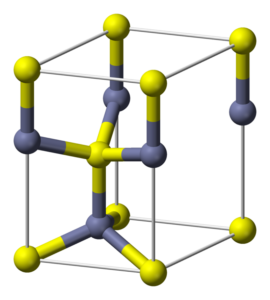
Representation of the wurtzite unit cell from Benjah-bmm27.
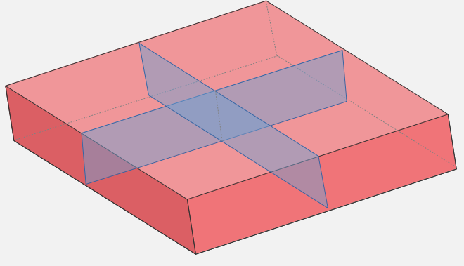
Align the Cleaving streets to the crystal
For successful cleaving it is very important to precisely align the cleaving streets and the scribe along the desired crystallographic plane. The wafer itself has a circle shape because it is cut from a cylinder (boule or synthetic crystal ingot) but the wafer manufacturer grinds a notch (called “flat”) that reveals the crystal orientation. The scribe tool must inflict the kerf exactly aligned with the crystal plane. For this purpose is very helpful to have a table with a very finely tuned rotational gear and a very tight angular lock position. To achieve acceptable results, you should be able to rotate the wafer and hold tight within 0,5° of the crystal plane. OptoSystem’s scribe and break tools have a motorized table with camera-assisted rotation adjustment. The tools automatically search for the flat and rotate the table with a resolution of less than 0,00035°. The mastery of the mechanical handling significantly increases the chances for high production yields.
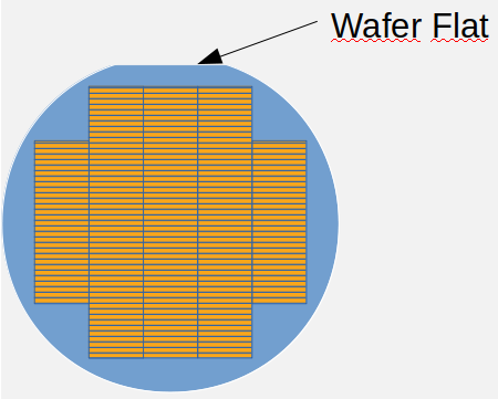
The notch on one side of the wafer indicates the crystal orientation.
Choosing the Right Scribing Method
The preferred process for singulating laser diodes is scribe and break, allowing the semiconductor to cleave along its natural crystal planes. The scribe inflicts a small mechanical damage that will become the starting point of the separation. By applying some mechanical pressure on the crystal plane, the semiconductor will fracture along its lattice planes starting at the scribed weak point. The desired result is two parallel mirror-like perfect facets and no collateral damage. There are specific challenges to each material system and different methods to do it. The most common method with laser diodes is diamond scribing for softer materials, such as GaAs and InP and laser scribing for harder materials, such as GaN. The diamond scribing applies pressure with a very sharp and hard edge and creates a median crack that propagates deep into the semiconductor. The laser scribing thermally ablates the semiconductor creating a deep and thin kerf but without applying mechanical pressure.
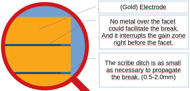
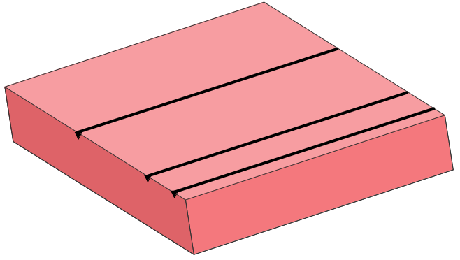
Model depiction of a semicondutor segment with cleaving streets that has been already scribed.
Do you like what you see?
We value your feedback, so let us know what you think!
Let us also know which topics you would like to see expanded.
Just give us a call, send us an e-mail or use the form to contact us.