CATEGORIES
Scribe And Break Process
The Overview
In this sub-wiki I try to depict the whole scribe and break process starting with a processed laser wafer and ending either with laser bars or with laser diode chips. The steps of stacking, facet coating and unstacking, as well as the optical inspection and the measurement are not part of this process description. Please note that each laser diode is unique and will require a dedicated approach. This is just a very basic overview based on the operation with Opto System tools and if you have specific questions related to your own products, you should totally contact us.
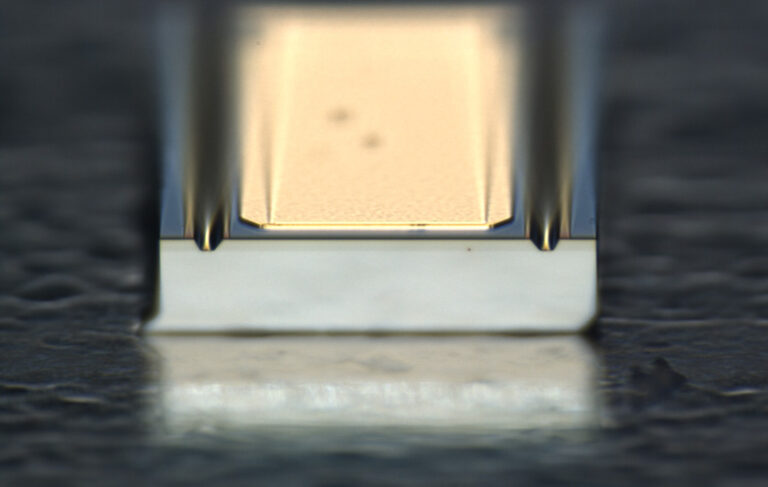
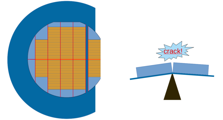
It is rather impossible to dice such smooth facets. They are cleaved in a similar way as diamonds are.
Preparations
After all the wet processes of the wafer have been completed the wafer is ready to be separated into individual laser bars or chips. Generally, the wafer is thinned to just around 100µm and on the bottom side the n metallic contact is grown with a sputtering or another PVD tool. In many cases, the p contact of the laser diode is on the top side and the n contact is on the bottom side of the diode.
Typical sizes for laser diode wafers are 2″, 3″ or 4″ and after being thinned to just 100µm, they easily bend and break. To ease handling and avoid unintended fracture, the wafers are placed on a sticky foil such as blue tape (it is actually blue for some reason), UV tape or other form of flexible tape that sticks to the wafer while being easy to remove.
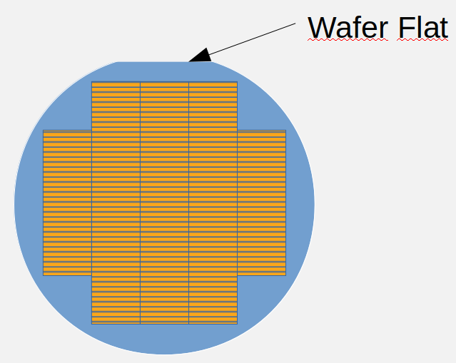
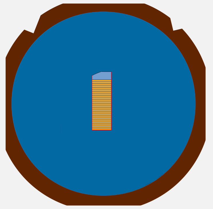
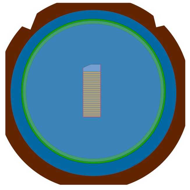
Top view of a wafer with completed laser diode manufacturing. The yellow stripes schematically depict the laser bars. In this example, the laser diode resonator would be oriented perpendicular to the flat. The streets between the laser bars have intentionally been left without metallization to ease the scribe and break process.
Frames to handle the tape with the wafer
Even for a wafer that is just 4 inches or smaller, its handling after thinning down to ~100µm is a delicate issue. During the next steps, the wafers are therefore placed on a sticky foil such as blue tape, UV tape or other form of tape that sticks to the wafer but allows to be stretched and to detach the wafer from the tape. The tape gives the wafer stability and the combination of both is easy to handle without breaking the wafer. The tape itself is attached to a thin frame. Different tapes will also produce different cleaving results. Opto System offers a variety of tapes and will help you find the one that delivers best results for your process.
The frame size is usually (at least) two inches in diameter larger than the wafer size. All frame sizes and exact dimensions follow an international standard. The frame material can be resin or metal. The frames can as well hold a barcode with information about the wafer they are carrying.
Frames have special features that ease automated robotic handling by autoloaders for instance. Frames perfectly fit in standard cassettes holding a maximum of 25 frames. Opto System offers optional autoloaders with almost all their tools.
Although frames are round, the specific patterns help distinguish their orientation that is usually related to the flat orientation of the wafer and hence the crystal orientation.
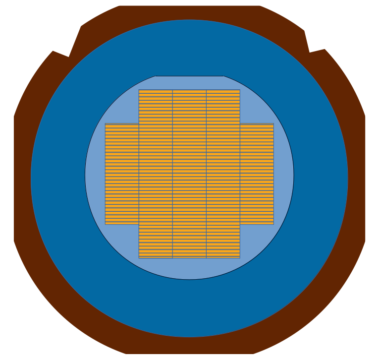
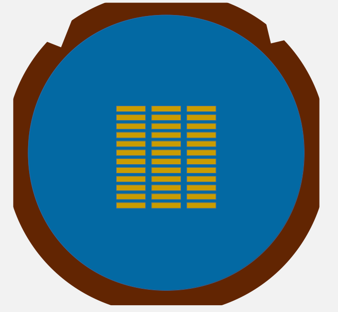
Top view of a wafer being held by blue tape and its corresponding frame. The brown color is arbitrary. There are metallic frames and resin frames in different colors. Note that the dents on the top side are different on left and right side, helping identify if the frame is upside down and its orientation.
Breaking the Wafer down in segments
The first step is to break up the wafer into smaller segments that are easier to handle. A laser scriber or a diamond scriber is used to place continous scribes along the borders of the wafer. In an automatic tool such as the the diamond scriber OSM-100TS, the frame with the wafer is placed in the machine, the correct processing program is chosen, and the scriber automatically recognizes the structures and places the scribes automatically in a moment. The same is true for a laser scriber such as the WSF-4000. When the scribing process is finished, the frame can be removed from the scriber and we see the result on the picture.
Since fractures tend to propagate along crystal planes, less damage on unintended areas can be expected if the segments are arranged along straigt lines that are parallel and perpendicular to the crystal planes, such as in the example in the picture. If your alignment is poor, you may want to consider upgrading your mask aligner.
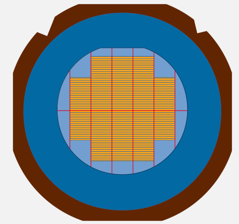
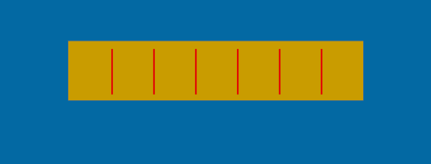
In this top view of a laser diode wafer, the scribes that divide the different segments are depicted with a red line. In real life, depending on the method used, they might not be visible without looking carefully.
This can be done manually
Breaking tools do not usually come with such big knives to act on a full wafer. But since the segments are comparatively large, the wafer is extremely thin and the scribes are continuous throughout the whole length of the aimed fracture, it is very easy to break the segments. As a matter of fact, they even might break while detaching them, but it is also possible to bend the tape over a sharp edge. Also the residual strain of the wafers could lead to their break by themselves once the scribe has been placed.
By peeling the wafer from the tape, the now individual segments can be placed on their own frames.
ESD protection measures can never be overstated but peeling plastic from delicate devices is such a situation when high currents can be generated if the standard ESD protections measures are not observed.
The picture on the left shows a top view of how the broken segments are detached from the tape by peeling the tape off. On the right side a side view of the tape holding a wafer is bent over a sharp edge. This bending strain, when applied on the right spot, forces the wafer to break along the previously created scribes.
Scribing for Cell-To-Bar step
After placing each segment (also called cell) on its own frame, the frame is placed again on the scribing tool.
The next step is to place small scribes in the cleaving streets. Depending on the material and the scribing method, different scribe lengths and patterns will be necessary. Either way, to obtain mirror like facets, the active area of the laser emitter should never be scribed. For more details on this step, see our sub-wiki on diamond scribing and on laser scribing as well.
Top view of a segment of wafer that is resting on a tape with frame when the scribes for the cell-to-bar process are set and when the segment is cleaved into individual bars.
Cleaving the bars
When the scribes have been placed, the frame is removed from the scribing tool and placed in the breaker. If you happen to own a tape cleaver, this is the step where you would use it. We describe here the standard breaking tool instead, which is Opto System’s most universal breaking tool that can be applied to virtually all breaking and cleaving processes:
A three point system will apply pressure along specific points to break the bars without allowing them to scratch on each other. The process is automatically controlled by a complex machine vision system with multiple points of view to make sure that the best results can be achieved with the minimum amount of force.
For the operation of the breaker, a mylar tape protecting the devices is placed on top of the wafer. The wafer is then placed upside down on the breaking machine, such as the LDH-100TSX. After selecting the correct program, the breaker takes over and moves the wafer segment on top of the support. A camera looking through the support makes sure that the scribe is located right beneath the cutter. In the next step, the cutter or knife hits the wafer from the back, bending the semiconductor, and the crystal cleaves along its planes. This is how the perfect mirror faces are generated.
On the picture the schematic operation principle of the breaker is shown from two different side views. The scribes are marked in red color. The top drawing would be looking at the laser bars directly into their emitting side while the bottom drawing looks at the cavity length of the laser bars from the side. In the bottom drawing the gap of the support is shown. The gap size can be adjusted depending on the geometry of the bars to improve results. The whole process is full automatic and very fast. The results are reliable and consistent.
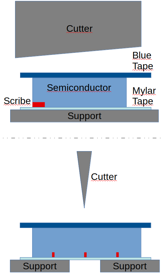
Breaker schematic operation principle.
Removing the scribes
A bit of fine tuning is needed for the specific processing of each material and specific edge emitter geometry and intended properties but sometimes the scribes are shaved off. This is easily done by applying a continuous scribe normal to the bar scribes. This is done right after the bars have been successfully cleaved and before expanding the tape. This process is normally only done for high power laser bars that are not further diced into individual chips.
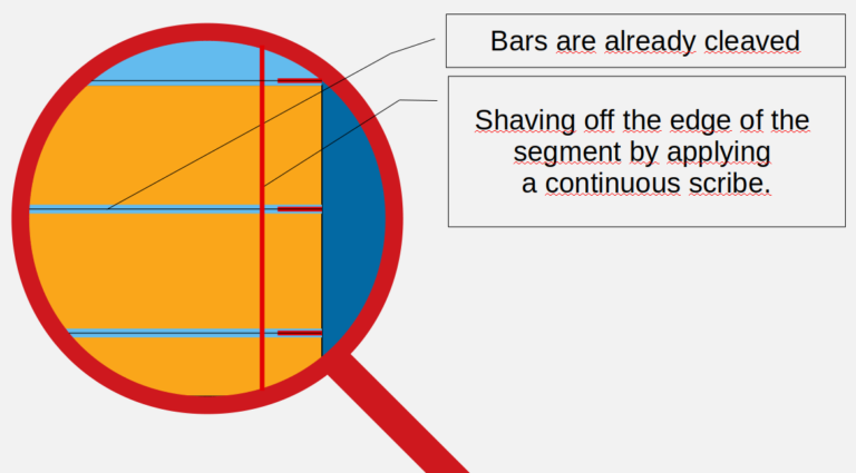
Microscope view drawing of the laser bars after scribe and break. The red lines show the position of the scribes. In this case this would be the typical pattern of InP or GaAs cells that are scribed and cleaved into laser bars. The vertical line shows the continuous scribe that was placed after the cleaving was successfully completed.
Tape Expanding
After the cleaving has been successfully completed, it is advised to expand the tape.
Expanding the tape and clamping a ring that snaps the expanded tape forces the devices to separate and you get a bit of handling space between them. This greatly helps to avoid further damage of the facets.
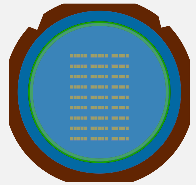
The drawing shows how it generally looks like after a successful cleaving and after expanding the frame tape on a ring. The ring is a circular snap device usually made of resin. The tape contained within the ring has been expanded. Now there is a small distance between the freshly created bars and they are easier to handle without damaging.
It is also possible from here on to cut the blue tape along the ring and only handle the ring. The frame can now be cleaned and be used with new tape on a fresh wafer.
Top view of a frame and a ring after expanding the tape.
Dicing Bars into Chips
If the bars should be singulated into separate chips, the next step is to dice the chips from the bars. In most cases, for laser diodes, this is done using the same equipment that was used to cleave the bars. In many cases there is a perpendicular crystal plane that can be used to cleave the chips. For laser diode chips though, the quality of the chip sides (other than the facets) is not too relevant and even a ‘dirty’ break is good enough for this process.
This step happens after the coating of the mirrors and in many cases, its optical inspection. The laser bars are placed on the taped frame forming an array either by hand or automatically by an unstacking machine. The frame with the laser bars is placed in the scribing machine. After selecting the right program, the scribes are automatically placed either by the diamond scriber or by the laser scriber.
Top view of a frame with laser bars arranged in an array for further scribe and break processing.
Scribing Chips
To ensure that all the chips will break, a continuous scribe is placed along almost the whole resonator length of the laser bar. A short gap to the facets is left non-scribed to allow a natural cleaving effect that will minimize the damage potential on the facet.
Close-up drawing of a bar scribed for chip singulation
Breaking Bars into Chips
After the scribes have ben set, the frame can be transferred to the breaker, where the actual breaking process will be done automatically after selecting the correct program.
The location of the bars on the frame ist critical and they must be placed in a region of the frame that the automatic scriber and breaker can access.
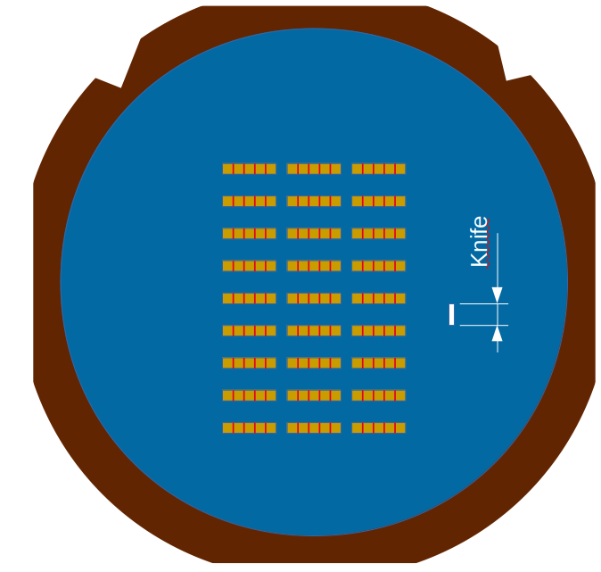
A bit tricky is the fact that in many labs only one breaker is used both to cleave the bars and to break the chips. Since the cutter or knife to cleave the bars must be pretty large, the bars cannot be placed too close to each other for the chip dicing if the same knife is used. It would otherwise unintentionally damage the neighboring bars.
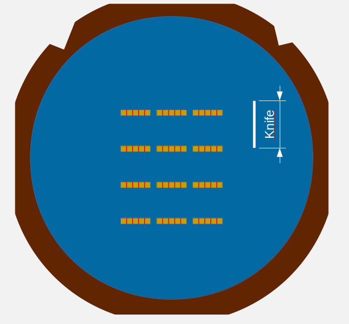
Top view of a frame with laser bars arranged in an array for breaking with a large knife.
Alternative with small knife
Either by changing the knife between processes or by having a dedicated tool with a small knife to perform the chip dicing, the amount of bars that are placed on one frame can be dramatically increased. In automatic machines this means a much longer time without intervention.
Changing the knife in a tool from Opto System is possible to be done by oneself but it does require a bit of practice.
However, Opto System’s breaker have a number of ways of dealing with this. The breaker LDH-100TSX has a mechanism to address with a small knife all bars placed in the area of 100mm x 100mm while the batch break mode will enable you to just break all chips in a column with just one single strike using the long knife!
Laser Bar arrangement on a frame for cutting using a small knife.
Expanding After Breaking
After breaking the chips, these are picked up by an automatic chip tester or other pick and place tool. Expanding the tape before the chips are picked up, can help this process.
Top view of a frame expanded tape after breaking the bars into chips.
Do you like what you see?
We value your feedback, so let us know what you think!
Let us also know which topics you would like to see expanded.
Just give us a call, send us an e-mail or use the form to contact us.