CATEGORIES
Confining The Photons
High Photon Density for Stimulated Emission
The stimulated emission is the key word here. A photon inside the semiconductor stimulates an electron in the upper band to release its extra energy in the form of a second photon. Coincidentally, the second and the first photon have the same energy and phase (coherent light). By (electrically) supplying enough excited electrons and photons (through confinement) the conditions for lasing arise. The sufficient supply of excited electrons is what is often known as inversion of states.
Beyond the threshold current, the inversion of states and the sufficient availability of photons kick loose the lasing state. Absorption processes and spontaneous (incoherent) photon emission are greatly overpowered by the stimulated emission. The semiconductor renders itself transparent to the lasing wavelength because in order to elevate an electron to the top side of the excited band (the lower states are already occupied by excited electrons), more energy is needed than the emission energy, that can use the shortest path instead.
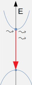
Stimulated emission bringing an excited electron from the bottom of the upper energy band to the top of the lower band. If this process is initiated by another photon, we speak about stimulated emission: Both photons will have the same phase. The opposite process (light absorption through an electron in the lower energy band) will require a higher energy because the upper band is already saturated with electrons (inversion of states).
the Laser Is a Light Waveguide
In an edge-emitting laser diode, the actual physical semiconductor bar is both the gain medium and the cavity that confines the light. A laser diode is as good as it is a good light waveguide. The required photon density is much harder to achieve if the photons can be anywhere in the crystal. Therefore, mirrors and high refraction layers that keep most of the photons bouncing back and forth into the tight gain medium provide a high concentration of photons in the gain region, encouraging stimulated emission (at the same phase). This has obviously also an effect on the beam pattern that the laser diode produces.
The high concentration of photons in the same phase is one of the characteristics that makes laser light so extremely useful for many applications. For stimulated emission a high photon density in the gain region is required, since these photons are the ones initiating the stimulated radiative recombination as opposed to a spontaneous radiation in a random phase that would create destructive interference.
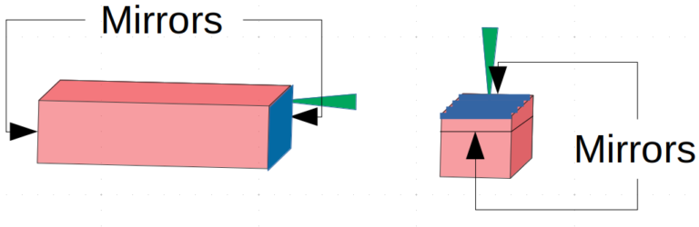
The physical dimension of an edge-emitter laser diode is the confining cavity, while in a vertical laser diode, the mirrors must be created as part of the thin film teposiiton during the heterostructure growth. In this depiction, the cavity of the vertical laser (right side) is extremely enlarged for visualization.
Vertical Lasers are often a Bunch
The low power of an individual VCSEL emitter is encountered by creating many VCSEL emitter cells next to each other. The result is a very affordable laser in which an array of hundreds of tiny lasers come together into a much larger chip which has a size of up to few mm² similar as that of an LED chip. VCSELs manufactured in this way do have an accumulated peak output power of several Watts at most but their emission area is obviously too large for some applications. Besides, there is a trade-off point at which increasing the semiconductor real estate does become more costly than manufacturing an edge emitting laser with the same or higher output power.
VCSELs are cheaper to manufacture than edge emitting lasers. Probably the main reason is that all fabrication processes can be made directly on the wafer whereas edge emitting lasers must consider and process the lateral walls of the components as well.
Whenever their particular beam characteristics and the power range is acceptable, VCSELs are used. Until now, there are no commercially available green or blue VCSELs, which poses an additional limitation for visualization applications. Yet, VCSELs are widespread in telecommunication and 3D imaging (to unlock a smartphone that recognizes it’s owner’s face for instance).
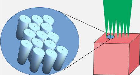
Vertical emitting lasers often combine a large number of emitters if the total required laser output is high. Unfortunately, this trick enlarges the emission area and is not suitable for applications where a single mode is needed.
Vertical Confinement in Edge-Emitters
In edge-emitting lasers the gain region are quantum wells in which the charge carriers are trapped in a state inversion zone that creates a very high gain region within the semiconductor. These so called quantum wells are manufactured with thin film deposition technologies, mostly MOVPE (metal-organic vapor phase deposition) methods. This does not directly limit the size of the cavity because the confining mirrors are actually perpendicular to the gain region. The light is vertically confined into the quantum wells by the deposition of layers with very high refraction index sandwiching the quantum wells (cladding layers) and forcing the light to go sideways instead. The light propagation in the gain plane can be further squeezed from the two dimensional plane into a one dimensional line by either passively confining the current injection to the injection street (current guiding) or by physically making the light propagation to the sides impossible (index guiding). This physical horizontal guiding can be achieved either by implanting high difraction dopants or by etching the gain region sideways of the resonator away creating a 3D structure like in a ridge waveguide laser. The mirrors at either end of the cavity are more or less automatically created by physically cleaving the semiconductor crystal. The cavity length is defined by the length at which the semiconductor is physically diced.
When higher power density is required, edge emitting lasers are usually preferable because their cavities are larger than that of a VCSEL. Due to the lack of appropriate materials, VCSELs are only available in wavelengths in the mm range up to dark red, which currently bans VCSELs commercially from applications needing visible light or an RGB system. Commercial visible laser diodes and UV laser diodes are hence always edge emitting lasers. Single mode lasers of few 10mW and more are usually edge-emitting lasers as well.
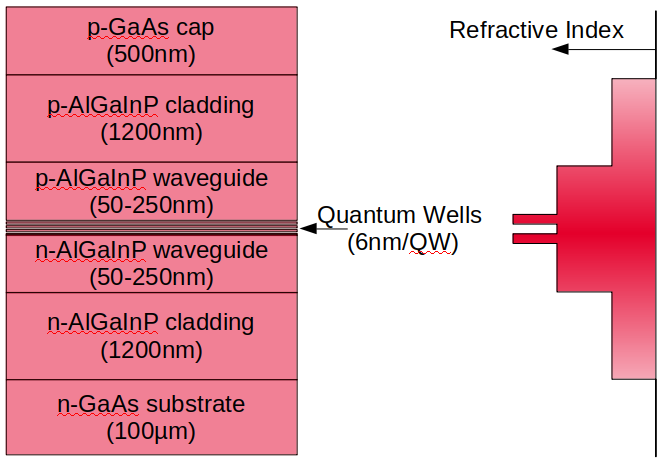
In edge-emiiting lasers the epitaxy structure also grows cladding layers to confine the photons in the gain region of the quantum wells. Bou Sanayeh, Marwan: Catastrophic Optical Damage in High-Power AlGalnP Diode Lasers. 2008.
Do you like what you see?
We value your feedback, so let us know what you think!
Let us also know which topics you would like to see expanded.
Just give us a call, send us an e-mail or use the form to contact us.