Types
The Key characteristics: A region with high gain and the optical cavity
There are many different types of laser diodes and as many ways to classify them. All lasers have key characteristics in common though: A gain mechanism and a resonating cavity. In laser diodes, the gain region is a material which is transparent for laser light and is able to amplify the light by means of electrical current or other photons of higher energy for instance. Laser diodes are often classified by the geometrical arrangement of the gain region and the resonating cavity: There are vertical emitters and edge emitters.
In vertical emitters the gain layers and the mirror layers comprising the resonating cavity are parallel to each other. Normally the laser light exits the semiconductor from the top face and the laser diode physically looks like a normal LED chip. As a matter of fact, LED and VCSEL manufacturing do have a lot in common. The gain region is sandwiched between two layers of reflecting mirrors that define the resonator. The mirrors and the gain layers are grown subsequently with thin film deposition processes. For this reason there is a thickness limitation of the resonator cavity that lies in the µm order of magnitude and hence the resonating cavity in which the light is amplified cannot be very large. To counteract this limitation, many individual VCSEL cavities are arranged in arrays and a grid of small VCSELs add up to considerable optical output power. The most famous vertical emitter laser are Vertical-Cavity Surface-Emitting Lasers (VCSELs) placed on smartphones for face recognition through 3D rendering but they have plenty of commercial applications.
The semiconductor materials used for laser diodes depend on the desired laser emission wavelength. The gain region is then created using different semiconductors and their common dopants. Typical are GaN for 405-520nm, GaAs for wavelengths around 800nm-1100nm, and InP for 1300-1500nm. More exotic applications include GaSb for even longer wavelengths.
If a higher output power is required but increasing the emitting area would have other detrimental properties, increasing the amount of emitters in an array would not be possible. Instead, the resonator length within the gain region needs to be enlarged. To this purpose, the geometry of ‘edge emitting’ lasers are often preferred over VCSEL’s. In edge emitting lasers, the gain region and the mirrors confining the resonating cavity are normal to each other. During the manufacturing process, the gain layers are grown on a wafer like in a VCSEL or LED with thin-film deposition techniques, but the mirrors are not deposited sandwiching the gain layers. Instead, the mirrors are deposited on the lateral walls of the semiconductor chips, that are created, when the individual chip from the wafer is diced. The physical lateral dimensions of the semiconductor define the resonator length, which can be in the mm range, hence at least 1000 times larger than a vertical cavity design. The laser light is forced to resonate perpendicularly to the gain layer and dwell in it, while it is been amplified, for a very long distance, which leads to a much larger optical power output than a vertical cavity design single chip. On the other side, their manufacturing is more complicated, generally involving cleaving the semiconductor to create facets that act as the laser resonator optical mirrors. Special care must be put on the facets to make sure that they withstand the extreme power densities. Special techniques are used, that involve a process of scribing, cleaving, stacking, mirror coating, unstacking, visual inspection of the facets and lateral electro-optical testing. High power material processing lasers are side-emitting lasers but also telecommunication lasers for data transmission are often edge emitting lasers as well .
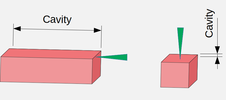
Edge emitting laser on the left and VCSEL on the right. In both depictions the gain region is a thin layer on the top. In the edge emitter the mirrors are located on the lateral walls while in the vertical design, the mirrors sandwich the gain region.
The most common gain region involves a heterostructure with an energy gap. When electrons recombine, a light photon is created.
The epitaxial growth of a stack of layers with changing thicknesses, doping and refraction index creates the heterostructure. A common substrate is a laser grade III-V semiconductor wafer because it matches the lattice constant of the desired crystal and allows to grow very pure layers with crystalline structure. At its core, the compound semiconductor forward-biased N-p-P heterostructure with a heavily doped P region traps the electrons and holes in the p region potential well creating a population inversion for the stimulated emission of photons. In the case of edge emitting lasers, this potential well, also called quantum well, is additionally sandwiched between layers with smaller refractive index (cladding layers) to guide the laser light along the gain region. In vertical cavity designs, instead of cladding layers, mirrors sandwich the gain region and create the resonating cavity. The cladding layers are necessary to increase the laser efficiency and suppress undesired laser modes. Additionally, the laser light can be laterally confined either by controlling the electrode width (gain guiding) and often by introduction of a laterally defined insulation structure (index guiding).
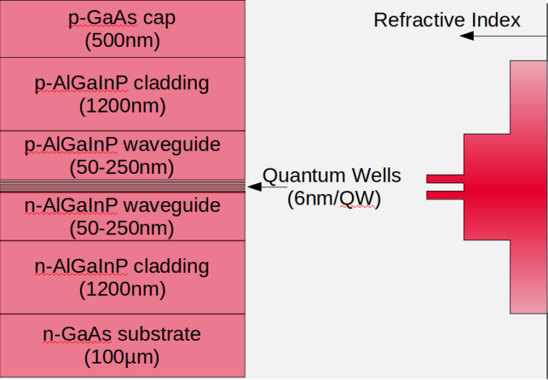
Simplified layer structure of a edge emitting laser. The substrate is few 100µm thick, the quantum well and the cladding layers are just a few 100nm thick
The critical layers to create the gain region and to confine the photons are grown on a substrate by using diverse thin film deposition technologies.
The actual quantum well and the cladding layers are all manufactured inside of a dedicated chamber. The tools for this process are called MOVPE (Metal Organic Vapor Phase Epitaxy), in which metal-organic gases, which molecules contain the semiconductor component and a more volatile organic compound, dissociate on a heated wafer by contact. The semiconductor atom deposits on the wafer while the organic compound returns to the gas phase and eventually abandons the chamber. By carefully controlling the gas composition, its partial pressure and the time it remains in the chamber, the different layers grow in their natural crystalline structure at the intended thickness and stoichiometry achieving a very high degree of homogeneity over the surface of the wafer.
Through the exact doping control, the band gap of the semiconductors is determined, which in terms, defines the wavelength of the emitted photons and of the laser. In the case of VCSELs, the two mirrors are either grownin the MOVPE step or grown separately and then bonded to the semiconductor chip. This inherent geometry poses a limit to the resonator length and hence the achievable power from a VCSEL.
The contacts to inject the electrical current as well as the lateral index guiding structures are deposited via evaporating and sputtering techniques in combination with UV – lithography and etching / lift-off steps. In many cases the wafer is thinned as well, often using CMP (Chemical Mechanical Polishing) to achieve a soldering surface free of scratches.
Do you like what you see?
We value your feedback, so let us know what you think!
Let us also know which topics you would like to see expanded.
Just give us a call, send us an e-mail or use the form to contact us.