CATEGORIES
Silicon Nitride thin film Properties and Use
The thermodynamic stable Si3N4 that can be created with standard thin film manufacturing procedures has a trigonal (α-Si3N4) or hexagonal (β-Si3N4) structure. Films are usually (unless grown epitaxially) an amorphous arrangement of tiny crystal grains of different sizes. The size and arrangement of the grains depend on the deposition and growth conditions. Si3N4 has a high melting point of 1900°C and it is chemically inert to most substances. Similarly to other ceramic compounds it has a very high hardness (8.5 on Mohs scale) and is an efficient migration barrier even to hydrogen.
Also, with its very low thermal coefficient, it does not develop stress when the device on which it has been fabricated is exposed to a wide range of temperatures. This also makes silicon nitride a good candidate for the manufacturing of thin membranes and even MEMS.
Silicon nitride is not only a very tough ceramic material but also an electrical insulator that plays a key role in microelectronics. It is often used as a gate in transistors and in other electronic components as well. If the manufactured film is dense and has no pinholes, it is also impermeable even to hydrogen.
Si3N4 is often used in combination with SiO2 because they act as an barrier to the etching agents that attack their counterpart, making patterning by chemical solutions relatively easy.
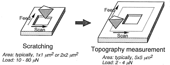
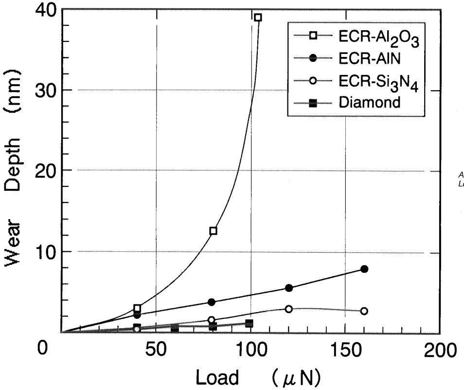
These AFM scratch tests were performed on ECR plasma sputtered films. Besides diamond, Si3N4 films are the hardest.
Optical Properties of Silicon Nitride
Si3N4 has a wide range of transparency from the UV to the IR and has a refraction index of n~2,01, which makes it very interesting as an optical coating for anti-reflective layers or as a component in multilayer dielectric mirrors. For this reason it is used as optical layer and encapsulation layer of solar cells, laser diodes, LEDs and OLEDs. The anti reflective coatings and dielectric mirrors help to increase their light coupling or extraction efficiency.
A further non-apparent advantage of Si3N4 over other layers as an optical coating is that there is no need to use oxygen during the process. In some applications, like the coating of edge emitting lasers or OLEDs, an oxidation of the underlying layers can have a negative impact on the device’s lifetime.
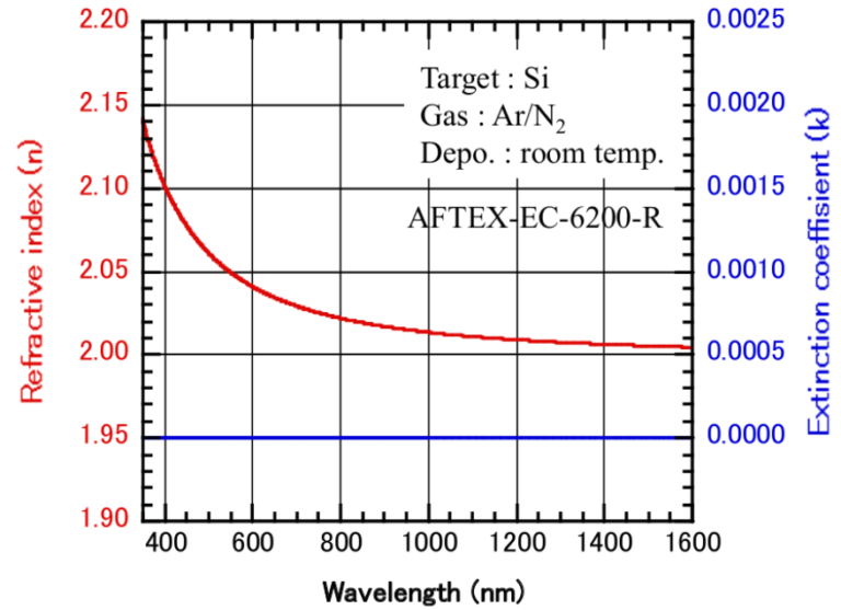
Optical properties of a thin film Si3N4 thin film deposited by a ECR plasma coating tool. Full transparency due to a full stoichiometric film free of hydrogen or an imbalance in the Si to N ratio.
Thin Film deposition Techniques for Si3N4
The film characteristics and properties can wildly vary depending on the method used. Most popular methods are commented here shortly.
- Chemical Vapor Deposition (CVD): Precursor gases are introduced in the chamber. The substrate is strongly heated and the gases react with each other at the contact of the hot substrate, creating the SixNy film and other gaseous species that are pumped out.
- Plasma Enhanced Chemical Vapor Deposition (PECVD): The heating of the substrate can be reduced and the stoichiometry of the SixNy can be influenced by introducing a plasma source to the deposition chamber. Otherwise it works like a standard CVD.
- Reactive Sputter: A silicon target is bombarded with argon and nitrogen atoms. These species are accelerated towards the substrate, where they hit with large energy and build a film.
- Electron Cyclotron Resonant (ECR) plasma reactive sputter: In this highly refined form of the reactive sputter system, the sputter plasma acting on the silicon is strong but the impact energy of the ions is much smaller. Hot electrons heat up the thin film and allow a high adatom mobility. The individual atoms in the coalescing film are enabled to find the lowest energy position and configuration. It is as close as it gets to an epitaxial growth with sputter growth rate.
All deposition techniques described here have in common that they are performed in a deposition chamber. Yet, the differences in the atomic structure of the film and its properties can be very large. ECR plasma tools are more complex than CVD or standard magnetron sputtering tools.
Coating Methods and their side effects
In CVD, the deposition does not deliver much energy to the growing film. The result is a thin film with a lot of interstitial spaces and pinhole defects. The precursor gases silane and ammonia react on the substrate leaving a considerable amount of hydrogen trapped back in the film. This deviation from a stoichiometric silicon nitride film also renders the film partially optically opaque and messes with the electrical properties of SixNy (often non-stoichiometric). Hydrogen atoms built into the silicon nitride structure serve as charge traps and modify the etch behavior of the film for post-deposition patterning.
The hydrogen that is released within the SixNy at a post-deposition annealing step does help with the passivation properties of the thin film though. To reduce the optical absorption, which is specially visible at short wavelengths, high temperature deposition and high temperature annealing post deposition is applied. With PECVD, low temperature deposition becomes feasible but this still implies using hydrogen containing precursor gases.For this reason, we often talk about H:SixNy films.
Reactive sputter deposition techniques deliver films that are denser and are manufactured without hydrogen (nor oxygen for that matter). Sputtering is the most common technique for optical thin films but there are important differences in the specifics of the tools and the thin film characteristics. Pure magnetron reactive sputtering or ion beam assisted simple sputtering tools tend to damage the underlying substrate and the films tend to be very rough.
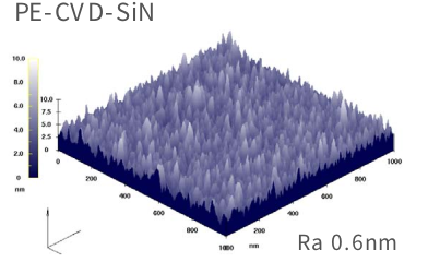
CVD coated films tend to grown in columns, leaving interstitial spaces and hydrogen from the precursor gases. PECVD coated SiN film roughness.
ECR Plasma coating of Si3N4
Silicon nitride films manufactured with ECR plasma sputtering are dense, stoichiometric, have no measurable hydrogen content and hence are transparent and deliver a refraction index ~2.01 close to the theoretical value from UV to IR across the visible spectrum. The ECR plasma sputtering method does not need to heat up the substrate, which is often a required specification to protect the devices. Besides, it is usually not necessary to anneal the films afterwards to improve the thin film characteristics.
In the ECR sputter plasma, a silicon target is sputtered with argon ions providing Si atoms into the coating chamber. The nitrogen gas is added through a separate line into the chamber. The gas flow and sputter power is carefully adjusted and regulated to achieve a stoichiometric film at a high growth rate. The transition between a poisoned and metallic mode target is in the case of a silicon target and reactive gaseous nitrogen less pronounced than for other reactive combinations.
The species of Si, SiN and N reach the substrate with relatively small kinetic energy of just few 10eV. This is enough to densify the growing film, knocking down columnar growth, while not enough to damage or roughen the underlying substrate. Also not enough for a significant sputtering effect on the substrate that would alter the stoichiometry and damage the structure of the growing film. On the other side, the ECR plasma delivers a considerable amount of energy in form of hot electrons to the growing film. This increases the thin film temperature and the mobility of the coalescing atoms that can move around to locate themselves in the spots with lowest energy. This creates ideal conditions for a crystalline smooth and dense thin film very early in the growth phase. If you want to see it with your own eyes, ask away for a test coating on your devices.
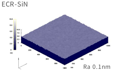
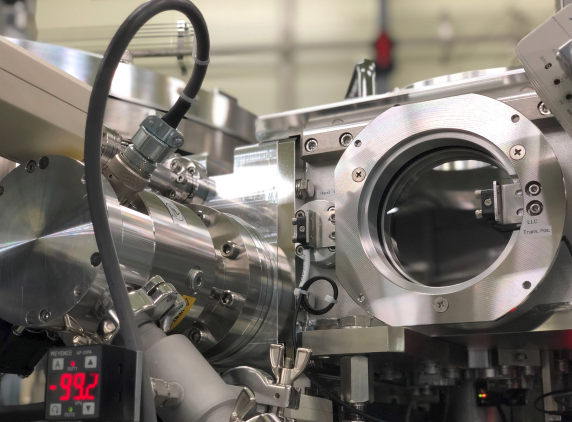
ECR plasma sputter coating of SiN with a ECR plasma coating tool delivers dense and smooth films from the very first nanometers.
Do you like what you see?
We value your feedback, so let us know what you think!
Let us also know which topics you would like to see expanded.
Just give us a call, send us an e-mail or use the form to contact us.