Search
Close this search box.

Opto System Visual Inspection Tool VVS2000

Highlights of the OptoSystem OptoSystem Laser Diode Chip Visual Inspection Tool VVS2000

Diode Facet Inspection.

100% optical inspection of the top side and both facets without picking up the diodes.

High Throughput.

The optical set up enables facet inspection withouth the need of chip pick and place.

For any chip geometry including laser bars.

Please talk to us about your chip or laser bar geometry.

Facet-inspection-VVF2200-Article

Vision Setup.

High resolution cameras, perfect lighting and intelligent algorithms find potential defects.

Technology Made in Japan.

Reliable and robust tools made in Japan with high quality materials for stable long term operation.

Full Automatic Function.

With an optional autoloader you can further extend the no-interaction operation.

Full Automatic Laser Chip Optical Inspection

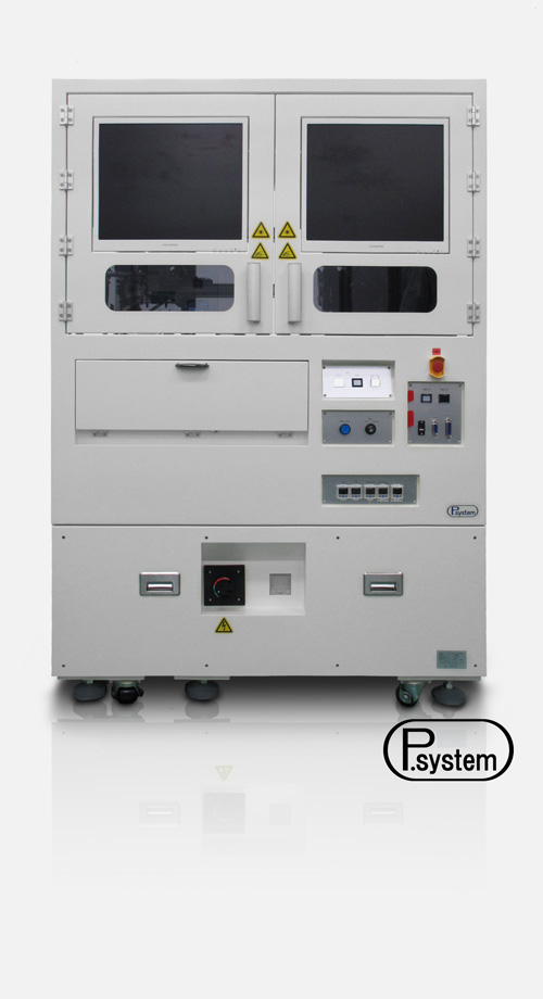
Description Opto System Laser Diode Chip Visual Inspection Tool VVS2000

The full automatic optical inspection VVS2000 is able to inspect not only potential defects on the top side, but thanks to a dedicated optical stage, also the facets of laser diodes. The geometry of the lasers is irrelevant, because the specialty of this tool is that the diodes do not need to be picked up from the tape. The optical set-up that looks at the facets from the side at an angle and a clever algorithm are able to identify potential defects of 3µm size or larger on the facets while defects of 1µm or larger are detected on the top side. The optics in the VVS2000 make the handling of the chips unnecessary, which saves precious time and increases the throughput. The pictures are analyzed with a state-of-the art algorithm and the pictures can be saved in a database.

FAQ

What about a machine that can do more than the inspection?

It depends on your situation: The VDVS3000 combines for instance laser bar unstacking and optical inspection, and the VVSP4000 not only has a more thorough optical inspection but also performs a sorting in different bins for immediate delivery to customers. The VVS2000 tool is the best option if you are just interested in optical inspection and the resolution of 3µm for the facets is good enough for your product because it avoids handling the chips and therefore makes it very fast. Most tools that OptoSystem delivers are custom made to meet specific requirements so do not hesitate to reach out if you have  a totally different configuration in mind.

What is the maximum resolution of the visual inspection?

We can adjust the camera amplification and resolution to your requirements but the challenge of not picking up the chips poses some limits on the optical inspection of the facets. Current optical setup for failure recognition on the facet achieves a minimum defect size detection of 3µm. The top side defects on the other side are already detected even if they are just 1µm size. The pictures are then automatically evaluated for defects and the chip is electronically labeled as good or bad depending on the criteria. The pictures that show the defects are saved in a HDD and can be reviewed later for recognizing eventual false negatives.

What happens when defects are idenfied?

The pictures can be saved in a HDD for an optional later validation through an operator. The identified parts are marked in a map data output so that in the following processing steps they can be ignored and scrapped. As an option we can have them physically sorted out directly at the VVS2000 as well. There is still the option of ink-marking the defective devices whereas this is nowadays a bit outdated and it carries the risk of cross contamination of adjacent chips. Depending on your situation, we either recommend the map data or the physical sorting-out.

Do you process my wafers?

Right now we do not have the capability to act as an OEM manufacturer but we are looking for partners to be able to do so in the future. If you want to try out how our tools work on your devices, please get in touch and send us some samples. We are eager to show off and learn about new applications. If you own OptoSystem tools and would like to offer OEM services, please get in touch too!

Why Opto System?

Opto System’s tools are built to last and very robust with a focus on performance and quality. Opto System has been around for for more than 40 years and has earned a reputation for excellent tools in the semiconductor industry across the world.

Who or What is Tomosemi?

TomoSemi is a manufacturer’s representative appointed by Opto System to promote Opto System’s products and to help customers in Europe since we are local.

Contact​

We value your feedback, so let us know what you think!

Just give us a call, send us an e-mail or use the form to contact us.