Search
Close this search box.

OptoSystem High Throughput AOI VVF4000

Highlights of the OptoSystem OptoSystem Laser Diode OptoSystem High Throughput Automatic Optical Inspection tool​ VVF4000

Diode Facet Inspection.

100% optical inspection of the top side and both facets (bottom side optional). Intelligent algorithms find potential defects and separates good from bad.

Two Stages For High Throughput

Enables detection of 1µm defects even though other parts of the tool are moving to increase the throughput. High resolution cameras and perfect lighting.

No need To Pick and Place

The frames are automatically drawn and replaced into the magazine and a map of good and defective devices is delivered within few seconds per device.

Full Automatic High Precision Optical Inspection For Device Facets At Top Speed

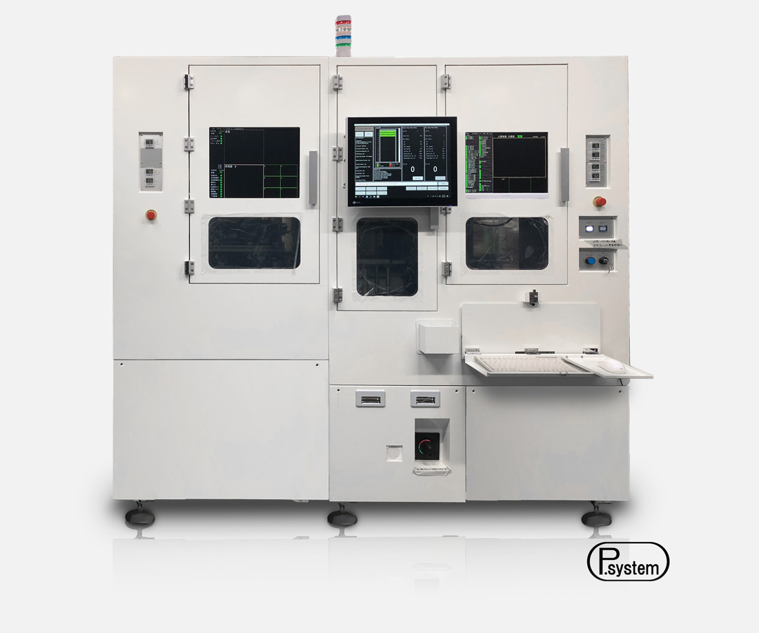
Description OptoSystem Laser Diode Chip Visual Inspection Tool VVF4000

If you need to control the facets of your devices as this is the case for edge emitting laser diode manufacturing, and you are expecting a high volume, this is the tool to get the job done at just few seconds for each emitter. Independently if you are controlling bars or single devices, the frames are automatically loaded. The p-side and optionally the n-side is controlled and both facets are inspected for optical defects as small as 1µm. Optical inspection is still a necessary step that is easy to do manually for small quantities but better done by machine vision for large quantities. This is our fastest machine.

FAQ

What do you mean by The whole facet?

The VVF4000 has been developed for our customers manufacturing high power edge emitting laser diodes in big quantities. Until now, in order to provide the required resolution, it was necessary to pick up the devices away from their carrier with the tool VVSP4000. If you need to sort your devices, this might be your best option. However, many times sorting the devices is just a waste of time and a map of the frames with the inspection result is just as good. In this case, with the new optical technology in in this VVF4000 it is possible to achieve the same level of inspection accuracy but at a much higher speed. This development allows to inspect the whole facet top to bottom at such a resolution that even defects as small as 1µm are reliably detected without wasting time sorting the devices.

What is the maximum optical resolution?

We can adjust the camera amplification and resolution to your requirements. Highest requirements for failure recognition on the facet side are typically 1µm for the p-side and facets. For the bottom side, since it is done through the tape it is sitting on, we can check deviations of the chip shape for instance. The bars or chips that are resting on tape are processed on two different stages simultaneously to increase the throughput. Multiple pictures are taken from all three sides. The pictures are then automatically evaluated for defects and the device is electronically labeled as good or bad depending on your criteria. The pictures that show the defects are saved in a HDD and can be reviewed later for recognizing eventual false negatives.

How does the bottom inspection work?

Since the bars are not picked up from the tape, it is not possible to take pictures of the bottom side of the bars directly. However, with this option, we can modify one of the stages and include an additional camera. While the P-side and facets are being inspected by the regular cameras, without interfering with these, the additional camera looks at the device bottom side through the tape it is sitting on. For this reason, it is impossible to distinguish reliably from bubbles between the bar and the tape, but it is possible to detect if the overall shape is not ok.

Do you process my wafers?

Right now we do not have the capability to act as an OEM manufacturer but we are looking for partners to be able to do so in the future. If you want to try out how our tools work on your devices, please get in touch and send us some samples. We are eager to show off and learn about new applications. If you own OptoSystem tools and would like to offer OEM services, please get in touch too!

Why OptoSystem?

OptoSystem’s tools are built to last and very robust with a focus on performance and quality. OptoSystem has been around for for more than 40 years and has earned a reputation for excellent tools in the semiconductor industry across the world.

Who or What is Tomosemi?

TomoSemi is a manufacturer’s representative appointed by OptoSystem to promote OptoSystem’s products and to help customers in Europe since we are local.

Contact​

We value your feedback, so let us know what you think!

Just give us a call, send us an e-mail or use the form to contact us.