CATEGORIES
Laser Scribing on GaN, AlN and Sapphire Substrates
Evaporate a Thin Incision with Laser Light
A laser beam is focused on the semiconductor to thermally ablate an incision. The kerf should be thin and deep to create as little damage as possible. At a subsequent breaking step through impact or by bending the semiconductor, it breaks along the incision. If the scribe is inflicted along a natural crystallographic plane, the semiconductor will cleave along it and the result will be a mirror-like surface.
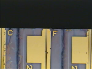
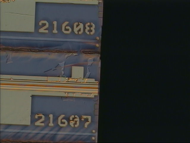
Top view on laser diodes that have been scribed by a laser beam.
The difference to a Diamond Scriber
The diamond scribing method may not easily provide satisfactory results on some materials. For these materials, a laser scriber is probably the best alternative. The scribing principle is totally different: The diamond scriber inflicts a crack by pressure but it might not be deep enough, lateral cracks might create problems or there is just not an appropriate crystallographic plane. The laser scribing method does not apply any pressure on the substrate but evaporates it thermally in a precisely localized kerf that is located in the streets between the dies.
In other words, it makes a thin and deep cut like a knife by evaporating the semiconductor with the focused heat provided by the laser light. Each substrate has a different absorbtion spectrum and the laser wavelength needs to match the absorbtion of the material that is to be scribed. The reduction of the cross section through the kerf defines the path along which the semiconductor will break.
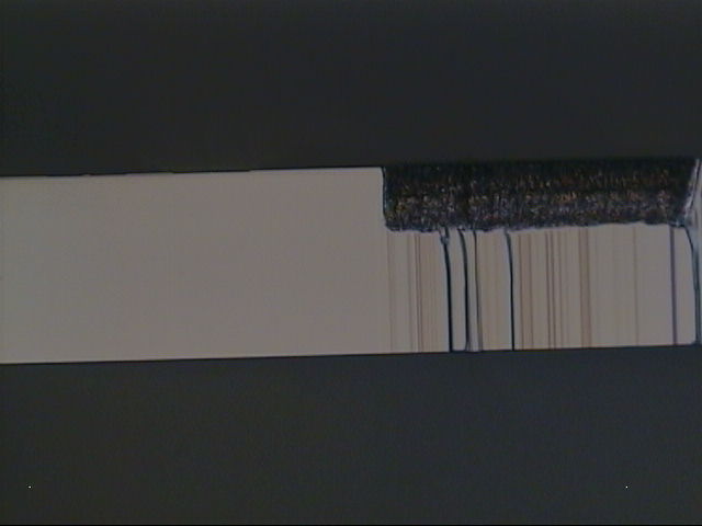
Side view of a GaN wafer after breaking. The facet completely follows the crystal plane and is mirror like. The scribe is clearly visible on the right side. Its depth amounts for almost one third of the total wafer thickness. Below the scribe, due to the finite width of the scribe, the crystal has cleaved along multiple planes, which is visible as a terraced facet.
GaN and Sapphire are challenging substrates
For this type of cut, in principle a mechanic saw could be used as well. But in comparison the laser scribing process does have a number of advantages over the mechanical saw. Foremost it is a dry process that does not need cooling water. There is no violent mechanical shattering that could create chipping and multiple micro cracks in the vicinity of the cut. Besides, the saw blades need to be exchanged relatively often and cannot provide the level of control and flexibility that a laser beam does provide.
GaN is the typical semiconductor chosen for blue and green laser diodes. Yet GaN is hard and brittle, and its wafers do still show some significant level of lattice defects. Therefore special tools and techniques are required to cleave GaN with a high yield. Crystal defects in GaN (and the inherent strain) are one source of fracture deviation and certainly one of the major reasons for unwanted terraces on the mirror facet. This problem is strongly increased by the hexagonal lattice of GaN (and Sapphire). The existence of crystal planes at relatively small angles to the cleaving plane helps the cleave street to depart from a straight line as soon as it encounters a dislocation or another kind of crystal defect. Since the cleaving tool does apply the bending force along the desired crystal plane the fracture path does return to the enforced plane but the overall result does entail terraces and a line that is not straight. The fracture changes often the breaking path from one plane to the other. The cleave street looks from the top like deviated from the intended cleaving street.
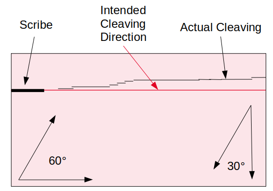
Top view of a scribed hexagonal crystal structure substrate. The thick black line represents the scribe. The thin red line represents the intended cleave direction. The thin black line represents the actual cleave after dicing the diode. The reason for the deviation is that dislocations in the crystal motivate the break to propagate along an adjacent plane for a very short distance. The total result is the impression that the substrate does not cleave along the crystal planes. The facet will look terraced.
Skip And Scribe
To minimize this, two techniques are applied. First, instead of using a diamond scriber, a laser scriber is used. The diamond scriber unintendedly creates not only a median crack along the desired cleaving plane but also chevron cracks and surface cracks along the hexagonal crystal planes that increase the chances of deviation. The direction of the scribe kerf created by the laser is entirely defined by the laser itself without being influenced by the crystal planes.
As an additional technique, the scribes are not only placed at the beginning of the fracture but all along the cleaving street like stitches of a sewing machine. This can be referred to as “skip-and-scribe”. The scribes cannot be too close to the portion of the facet that will become a dielectric mirror because then the facet would not be smooth. Other than that, the intermitent scribes are set all along the cleaving line.
Using a laser scriber and the “skip-and-scribe” method delivers high yields for GaN despite its challenges. Beneath the laser cut, due to the width of the kerf itself, the surface shows a lot of terraces but these heal out quickly in the area where the crystal cleaves naturally. To avoid deviated cleave propagation due to the high amount of lattice defects on GaN wafers and by the inherent strain, it is customary to scribe along a dashed line giving the cleave propagation a strong directional guidance.
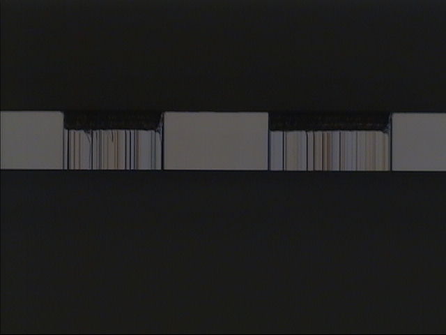
Side view on a cleaved GaN wafer. The facet reveals the portions where a laser scribe has ben set and where the natural plane cleavage has delivered mirror-like facets.
Laser Power Control
The reduction of the cross section could be done with a mechanical saw with a continuous cut along the street at a certain depth but only a scribing laser allows to easily create a dotted or dashed line pattern. The facet portion becoming a mirror should not be damaged by the melting action of the scribing laser but should be allowed to cleave along the crystal plane by itself instead.
The wavelength and type of the scribing laser is specific to the material being cut. Pulsed operation allows us to localize the heat very precisely while minimizing the damage of the adjacent areas. The re-deposition of the ablated material can be controlled to a certain extent by adjusting the laser parameters and its guiding through the substrate. The depth of the cut can be controlled by the laser power and to a certain extent also by multiple beam scanning.
Side view of a cleaved GaN substrate. The area that has been scribed shows terraces because the kerf has a limited width.
Not Overdoing it
With increased laser power, the risk of unwanted cracks due to thermal expansion is also increased. It also might increase the amount of material re-deposition. Therefore a careful choice of parameters is recommended.
The streets should be smooth and kept free of metallization to avoid unwanted scattering and reflection of the laser beam. An alternative could be to irradiate the substrate from the bottom instead. The implementation of top and bottom cameras can help align scribing on the bottom while monitoring the position on the top side or vice-versa.
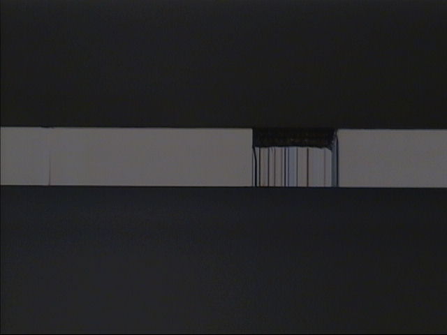
Top view of a laser scribe in a GaN substrate.
Picking the right Wavelength
OptoSystem’s popular choices are a nanosecond pulsed laser at 355nm for GaN and a picosecond pulsed laser at 532nm for scribing of Sapphire, both with many flexible parameter settings for process optimization. The laser scriber uses a state-of-the-art vision system with several cameras to identify the wafer structures and the scribe streets. The stage automatically rotates the wafer and aligns with the structures parallel and orthogonal to the wafer flat with high accuracy within 1°. The laser places the scribes in full automatic fashion at the desired wafer locations within 1 µm and with the desired intensity and length. The laser light is focused to a small spot of just few micrometers to reduce unnecessary damage. There are redundant interlocks and shielding according to standard regulations to protect the operators in the working environment from laser light reflections. The tools are robust and are already in operation partly for more than ten years with very little unplanned maintenance.
Laser scriber WSF 4000 from OptoSystem. A market leader from Japan for laser scribers.
Do you like what you see?
We value your feedback, so let us know what you think!
Let us also know which topics you would like to see expanded.
Just give us a call, send us an e-mail or use the form to contact us.