CATEGORIES
False Positives
And False Negatives
When devices are classified according to measurement results, there is the classification in positives and negatives. The positives are said to be fit to be delivered because they meet certain criteria according to a set of rules. The negatives will be sorted out and discarded because they do not meet at least one of the criteria from the classification rules. This applies to optical inspection and to any kind of measurement or diagnostics.
Due to the imperfect nature of the measurement procedure, there will be also ‘false positives’ and ‘false negatives’. These are respectively parts that are wrongly believed to have passed the test and those that are wrongly believed to have failed the test.
If the number of false positives or false negatives is high, there is a problem with the measurement system that needs to be addressed.
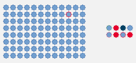
The laser diodes on the left have been sorted to be ok (positves), while the laser diodes on the right have been sorted to be not-ok (negatives). One laser diode is wrongly sorted in each side. In the left it is a false positive and will likely fail after delivery. On the right there is also a false negative: A laser that will be sorted out, although it seems to be ok.
Strategies for Improvement
In the case of optical inspection, a bad performance can be checked by re-running the same set of samples through different measurement systems and comparing the results.
If the poor result with a high amount of false positives and false negatives has been produced by a group of people evaluating the pictures, the solution could be to provide more training, reducing the inspection time per person and increasing the amount of short breaks.
If the measurement system is an automatic optical inspection system, the analyzing algorithm needs to be improved.
Manual optical inspection delivers more errors if done for a long period of time.
Algorithms take over
A much better strategy in semiconductor production is to let a machine do most of the job. The inherent handicap of algorithms can be encountered by limiting the optical view to easy geometrical shapes, improving the contrast with appropriate lighting and increasing the picture quality altogether.
In semiconductor manufacturing, most pictures look pretty much the same and looking at them for hours becomes boring. Both factors actually put the machine vision system on an overall advantage over manual visual inspection by a human.
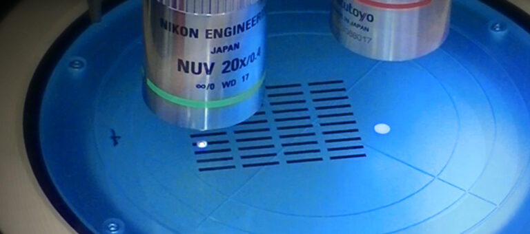
An optical inspection tool by OptoSystem automatically takes pictures and performs the classification of a laser diode or other device that has a visible defect (and which) or if it does not. There are various tool setups available to perform this job.
High resolution images and an algorithm can be more efficient in identifying optical defects than humans if the quantities are so large that a human would get bored.
Optimizing The Algorithm
To implement the necessary algorithm to perform the classification, the client sends several semiconductor devices to OptoSystem used for the learning step. Ideally, this training set has a large population of various types of defects that likely appear in device production.
To verify the precision of the algorithm in a second step after optimization to the devices used in the learning step, a random fresh set of new devices not used during the training step is sent through the machine and the classification is compared to human eye results to calculate the number of false positives and false negatives.
There tends to be an inverse relationship between the number of false positives and false negatives, where it is possible to reduce one at the cost of increasing the other.
The target is to reduce the number of false positives to zero to avoid passing defective devices to the end-user.
Some fabs choose to do a re-evaluation of the classified negatives by the human eye to increase the production yield. This can be done with the pictures that have been saved in the HDD whenever it is convenient.
Since the amount of negatives is usually much smaller than the number of positives (and there is always something “interesting” to look at) the workload and failure rate for an engineer is usually low enough and a good trade-off of invested time and recovered false negatives that increases the production yield. It is a good way to have a closer look at production fluctuations as well. Identifying repeating failure modes is the first step in addressing and correcting them.
In most cases, the algorithm can be expanded to new device types by yourself although OptoSystem’s staff would be happy to assist.
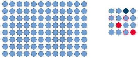
In this example there are no false positives but the amount of false negatives is higher. The positive tested can be delivered without passing on defective devices. The negatives are a smaller amount and can be either scrapped with little loss or double checked by a human eye to sort out the false negatives and increase the production yield..
What to look out for
The active area region of the mirror on an edge-emitting laser diode is especially important. Cracks on the semiconductor leading to the active region, delaminating mirror or mirror holes, chipping, facet steps, striations or large particles can be severe defects.
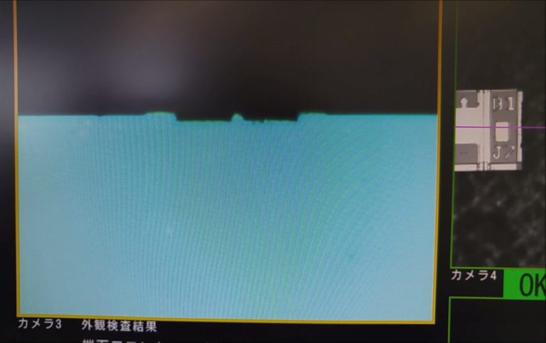
These types of defects are relatively easy to be identified by an algorithm. The algorithm generates a data table for production quality evaluation.
Some particles can be subsequently removed but the other failure modes on the mirror or in the semiconductor are likely irreparable and the whole bar or diode is declared negative.
On the p- and n-sides deep scratches and particles are typical failure modes. Deep scratches could lead to a short-circuit if they cut through the whole heterojunction. Large protruding particles that are baked-in will likely make problems at the soldering step, applying too much mechanical pressure on the semiconductor crystal and will likely crack the device in two. If the mechanical stress is not sufficient to create a crack it could bend the energy states in the semiconductor and create a nonradiative recombination center in the resonator that will overheat and either degrade the laser or cause its local meltdown if the heat is large enough.
The algorithm identifies these potential problems and measures the size of the particle or scratch. These parameters can be defined to discern if the laser diode should pass the optical inspection or not.
Do you like what you see?
We value your feedback, so let us know what you think!
Let us also know which topics you would like to see expanded.
Just give us a call, send us an e-mail or use the form to contact us.