Although we strive for it, it is impossible to manufacture 100% perfect chips. It pays off, at several steps, but especially before moving the chip towards assembly, to inspect carefully and reject defective chips. However, there are visible defects that only have a cosmetic effect but do not impact operation or lifetime. Depending on the size and nature of the defects, dedicated hardware such as amplification lenses, special cameras and illumination is required for detection. The most accurate judgement system is the human eye, but humans become bored easily and start to do mistakes after just a few chips. An automatic tool will locate the chips on tape and move the relevant parts to the imaging stage, then will apply a number of logic rules to sort out defective chips. Let’s see the basics.
The hardest part needs to be done beforehand. During the design of the chip, critical deviations from the ideal and their effects on performance and lifetime must be considered. A helpful way to look at a chip is to determine regions of interest and to identify them on the surface of the chip. Additionally, the fab can point out which defects are most prone to be expected depending on the manufacturing method. In the example on the right you can understand why some areas need a special treatment. Your chip will be different but will follow a similar principle. Each region has a technical reason to be on the chip and the visual inspection requirements will be specific to it. This also determines the kind of physical equipment that is necessary. For instance if 1µm particles or larger are to be detected, equipment with a resolution of 0,3µm is necessary.
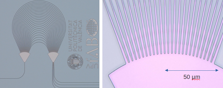
For this AWG (Arrayed Waveguide Grating) on the photonic chip the standard magnification is sufficient to identify large scratches, particles or defective metallization. However the FPR (Free Propagation Region) must be inspected with a larger magnification to check the separation of the waveguides. Image courtesy of UPVfab, Valencia, Spain (link)
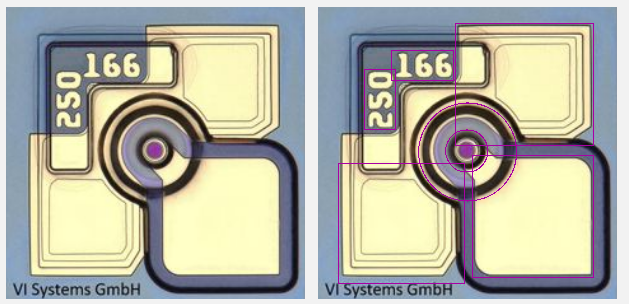
In this exemplary VCSEL chip, just with a single image shot, many different areas are inspected for critical problems. While a small particle on the bond pad might not pose a problem, the same particle size on the aperture might be a reason for rejecting the chip. The OCR reads the chip ID (in this case 250 and 166) and saves the gained information together with the chip ID for a potential future analysis.
We define the special areas of interest where defects should be sought for. The automatic inspection algorithm will search for particles, scratches or defective features on each area in which specific parameters can be set. As a result, not only the chip will be determined to be visually OK or a reject, but if a reject, also the reason why.
Image courtesy of VI-Systems GmbH (link)
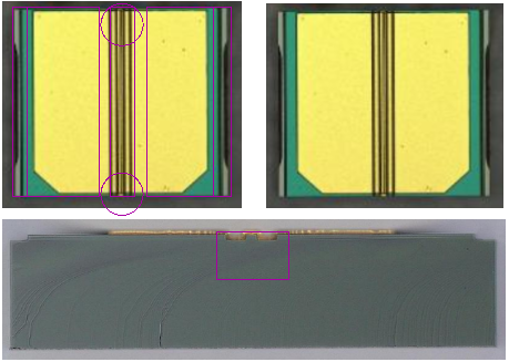
For edge emitting laser diodes, an additional technical challenge must be faced when doing optical inspection. For most devices, a 2-D top side inspection is sufficient. But one of the most critical features of this type of devices is actually located on the lateral side (facet) of the device. Hence, the top view inspection needs to determine where exactly the laser light will exit. In this example on the next figure it is easy to figure out due to the clearly visible position of the ridge. The tool then drives a camera to exact that position but looking from the side. The facet is generally inspected for shell cracks from the cleaving or particles on top of the emitter. The lateral size of the ridge or defective metallization could be specific features for edge emitters yet easy to verify with an automatic inspection tool.
Top view (standard) and facet view of a typical edge emitting laser diode. The automatic optical inspection finds and inspects the regions of interest for diverse defects.
Image courtesy of the Institute of Microelectronics and Photonics
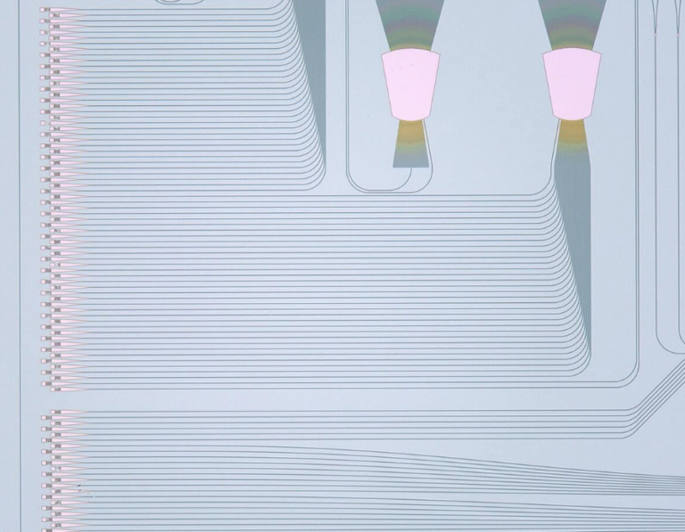
Depending on the size of the chip and the required inspection resolution it will be necessary to move the chip several times and take many pictures. This does not pose a technical problem and there are ways to reduce the inspection time. However, more images to inspect do generally mean a larger inspection time. Our tool is able to precisely move and keep track of every position despite needing to stitch several pictures into one big image of the whole chip. The image on the right has a lateral size of several millimeters yet the details that need to be inspected go down to few µm.
Photonic Chip showing multiple structures. Image courtesy of UPVfab, Valencia, Spain (link)
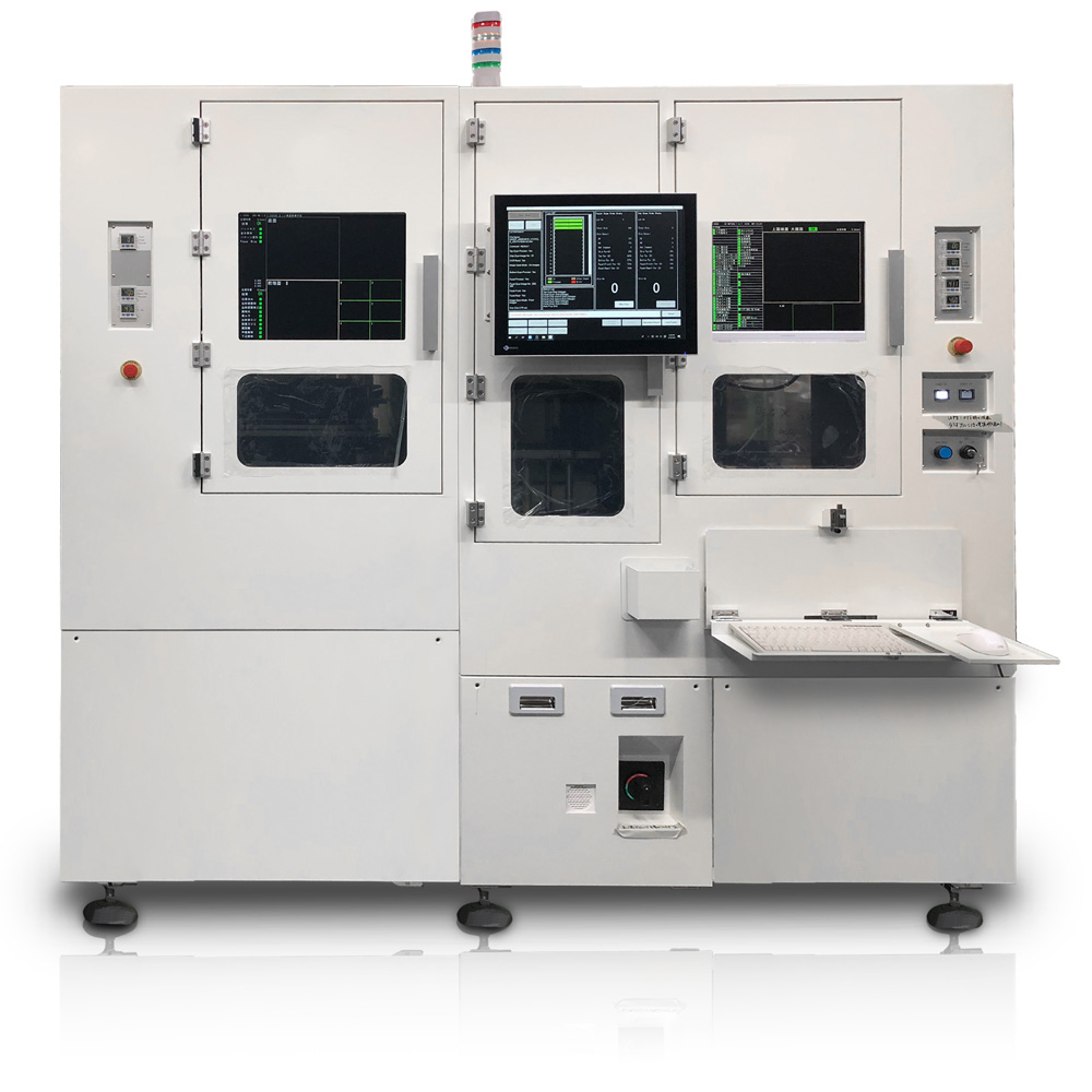
OptoSystem’s offers a large variety of tools for automatic optical inspection. Either tools that do not pick up the chips yet are able to take pictures of the facets of the devices. Or tools with sorting capability in which the good chips are automatically arranged in a new frame or directly into GelPaks. In the first case, without touching the chips, the process is very fast and adaptable to diverse chip geometries. In the second case, the images are taken either on the fly while being sorted or on a dedicated inspection stage with very high precision while adding an additional sorting capability. Check these options on our webpage for inspiration and then tell us more about your actual requirements: Our specialty is to manufacture custom tools.
We value your feedback, so let us know what you think!
Let us also know which topics you would like to see expanded.
Just give us a call, send us an e-mail or use the form to contact us.