CATEGORIES
Old School Cool:
Rule-based Recipes
Despite the evolution of Artificial Intelligence (AI) also in the field of visual inspection, there are many advantages to traditional rule-based recipe making: The rules are easy to understand and the outcome foreseeable for the engineer making them. The minimum number of samples required to verify the rules is very small and if your chip design changes, you don’t need to start from scratch, but can very easily adapt the existing recipes to match to your new design. The processing time even with relatively basic computing hardware is very small and you keep your IP within your own company without the requirement of trusting external data clouds. AI does have a very interesting field of application that we will discover later.
Checking for potential defects systematically
The way that inspection tools work is by following a number of steps that are programmed in advance. The tool follows a practical sequence that checks one rule at a time and one after another. Normally, this is something happening behind the scenes but it is helpful to understand. The chips, or parts hereof are first identified by a low-amplification camera and their locations are met. Then, after an automatic alignment and position-calibration process, the first picture is taken. That picture is then used as the object of analysis of a separate inspection program that follows the steps that we will describe with examples below. All these complex items are multifold, yet happen unnoticed, sometimes at a fraction of a second.
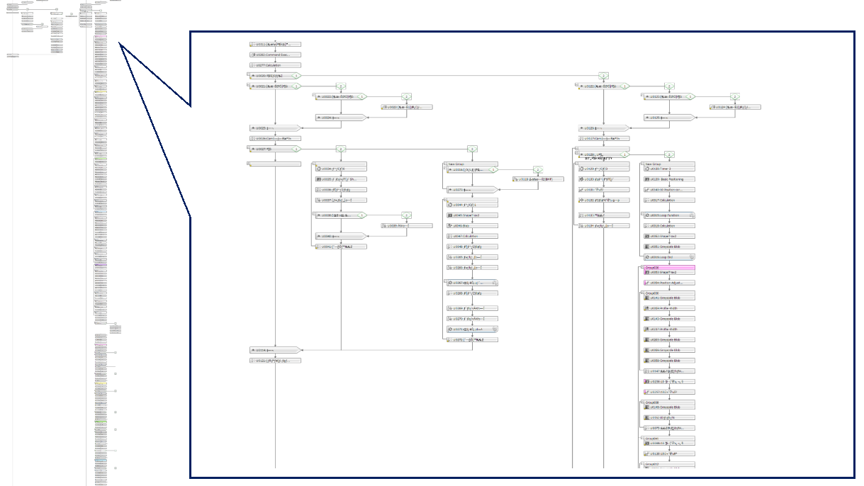
Excerpt of a process diagram for a simple optical inspection program checking for the different criteria of a failure catalogue for a specific chip family.
Applying Filters
It is very easy to define a region of interest. For instance on the example on the right, we define the large gold metal area as our region of interest but we exclude the central region. Masking out certain regions is done out of various motivations. This is just an example.
The next step is, depending on what you are looking for, to process the color and pixels of the image to highlight the sought features and to reduce noise. There are many different predefined ways to do it and they can be combined indefinitely delivering a huge spectrum of tools. In Opto System’s tool, even without any knowledge of image processing it is very easy to adjust to achieve different results on a user friendly GUI.
In the depicted figure, the yellow area (gold p-contact) is turned white while anything else is turned black. Any variation from a perfect surface is strongly highlighted and helps with the next step.
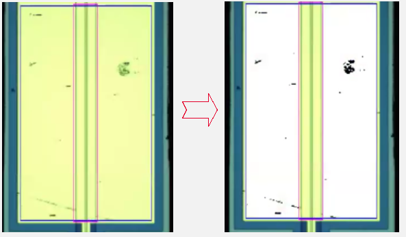
This image of the top side of an edge emitting laser diode is shown in its original colors (left) with two drawn rectangles to mark the regions of interest and the masked regions. The right side shows the same image after the marked regions have undergone a binary filter to highlight scratches and dirt.
Detecting Dirt
Particles can be either on the surface, ingrown, or leave a mark because they were there during a lithography step. Depending on where they are, their size and sometimes their height, they can create problems afterwards. A common parameter is the overall size of the particle, that may not reach a certain threshold or the device will be marked as faulty.
So how does the vision software work? It quickly scans over all pixels and starts counting those that stand out from a baseline of their surroundings. That is basically in a nutshell the most basic procedure. By then counting all pixels that belong together, the size of a lump or particle is determined. In the settings for this detection rule you can easily set the maximum allowed size for each specific region. It is very easy to do.
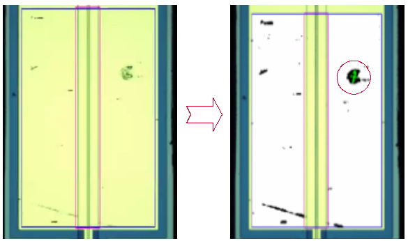
The left side of this image is the same as above. The right side shows that the vision software has identified one particle (highlighted with a red circle) that matches the rejection criteria because its total surface is larger than the threshold.
Detecting Scratches
Scratches are easy to be detected as a different type of damage. In most cases they are the result of improper handling and sometimes they are easier to reduce during manufacturing than particles. Therefore it makes sense to understand what percentage of your chips show scratches. However, most scratches are harmless and just a cosmetic imperfection. Especially on highly reflective gold they tend to look more dramatic than they actually are. However, when they are deep enough, or cross very sensitive areas, they may become the reason for an undesired electric shortcut.
The vision software will scan over the surface searching for pixels that stand out from their surrounding baseline. The software not only counts the total area that is covered by the aggregated pixels standing out, but also determines the length and width as well as the direction of the lump. It is also here very easy to set the parameters that lead to an unacceptable deep or long scratch.
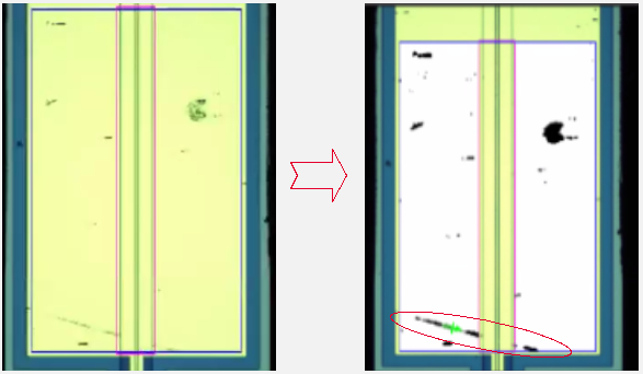
The left side of this image is the original. The right side shows that the vision software has identified one scratch (highlighted with a red circle) that matches the rejection criteria because its length is larger than the threshold. In this example the black and white filter and the parameters have been deliberately exaggerated to reject a chip because of an otherwise probably harmless thin scratch.
MEasuring Dimensions
In high frequency circuits and also for waveguides, narrow grooves and other difficult to manufacture sophisticated structures, a special attention is needed. Manual systems require the use of scales to measure a certain distance. In a machine, the distance has a constant mathematical relation to the amount of pixels that are found in a direction. For the machine it is quite easy to find two lines (encasing a groove for instance) and to measure their separation. In the parameters we can enter the range that is within reasonable manufacturing tolerance. The inspection machine marks then those with a too large (or too narrow) groove as rejected chips. Since the procedure is the same for any chip with a ridge design, by changing the threshold range, different designs can be processed with very little effort on the process engineering side.
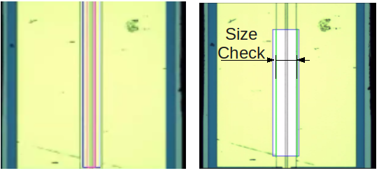
In the left image we have marked the ridge area in the center. In the right image we see how the filter highlights the lines. We can measure the distance between the outer lines or the inner lines. For the sake of the explanation we have chosen the outer lines but this can be done with very small dimensions that would not come out clear to see on the image displayed here as an example. The exact measurement is the data output.
Do you like what you see?
We value your feedback, so let us know what you think!
Let us also know which topics you would like to see expanded.
Just give us a call, send us an e-mail or use the form to contact us.